Forging the Future of Library Verification with AI-Powered Custom IC Design and Verification Solutions
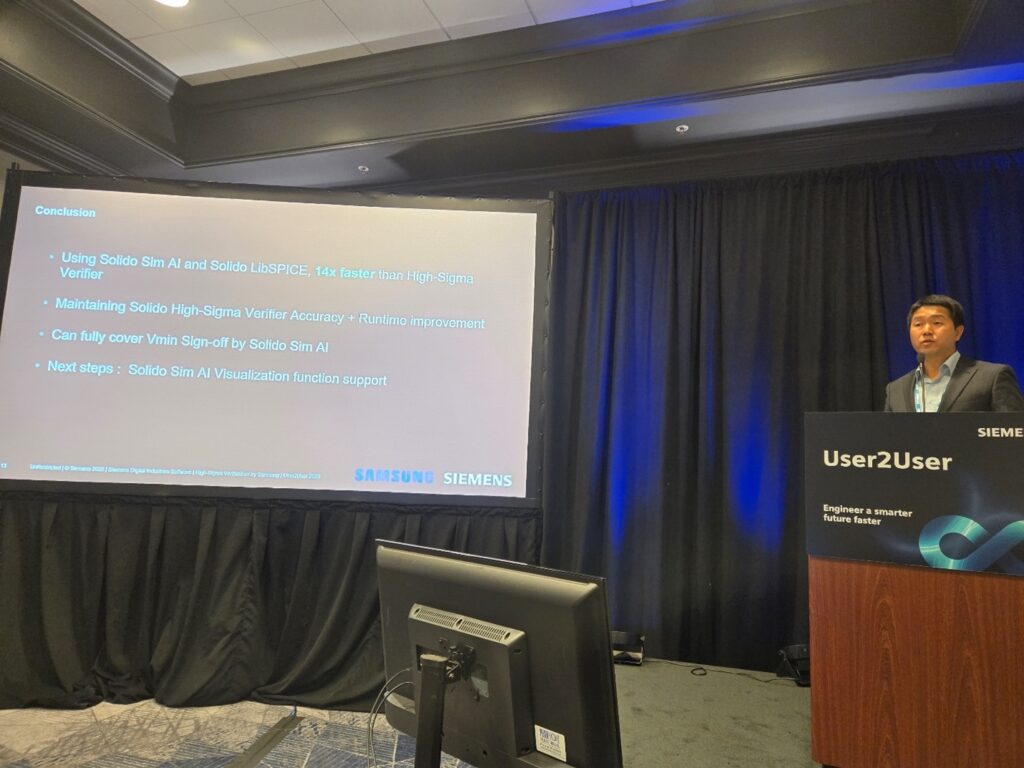
In a compelling presentation that captivated audiences at the Siemens User2User North America 2025 Conference, Dongsuk Lee, Principal Engineer at Samsung Foundry, unveiled how the powerful collaboration between Samsung Foundry and Siemens EDA has resulted in a groundbreaking methodology to speed up standard cell library verification by 14X over conventional approaches.
This presentation showcased the remarkable progress made recently by Siemens EDA that underscores the transformative power of AI in chip design, without compromising accuracy, speed and practical usability.
Transforming library verification
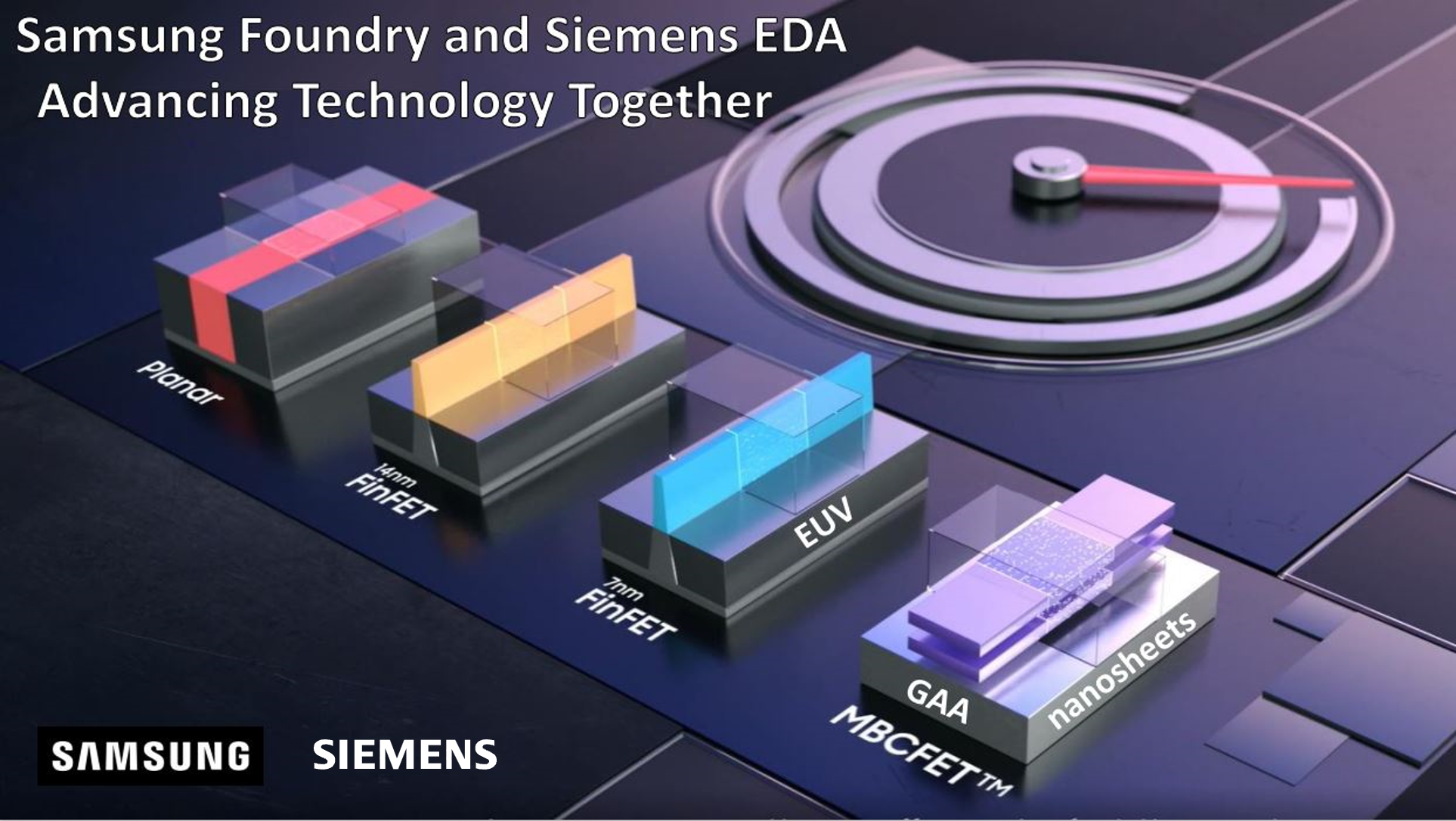
In an industry where nanometers matter and every picosecond counts, Samsung Foundry stands at the forefront of technology. From the innovative Fully Depleted Silicon On Insulator (FD-SOI) to cutting-edge Gate-All-Around (GAA) technologies, their portfolio covers a broad range of process nodes supporting a vast array of applications. With great technology comes great verification challenges – and this is where the magic of the Samsung Foundry and Siemens EDA partnership truly shines.
AI: the game-changer for library verification
“Time is quite literally money,” emphasized Mr. Lee, who has over 15 years of experience in analog and mixed-signal circuit design, highlighting a universal truth in the semiconductor industry. Enter Siemens EDA’s advanced AI-powered solutions: Solido™ Sim AI and Solido™ LibSPICE, part of Solido™ Simulation Suite. These aren’t just incremental improvements – they’re significant advancements in verification technology. The results? An impressive 14x speedup in standard cell library verification while maintaining high accuracy levels.
Breaking down the breakthrough
The numbers tell a compelling story. Traditional methods required nearly 1.5 million Monte Carlo samples, which would have taken ~ 8 months to simulate an entire library. Siemens EDA’s AI-driven approach changed the game entirely. The new solution delivers:
- Dramatic reduction in simulation samples by 80%, thereby reducing the total turn-around time (TAT) to 18 days for verifying the entire library
- SPICE-accurate high-sigma verification with +-0.1 sigma accuracy
- One-click automation replacing manual processes
A partnership built on innovation
This collaboration goes beyond typical vendor-client relationships. Samsung Foundry and Siemens EDA are co-creating solutions that address real-world challenges. The development of the Solido Sim AI parameter sweep flow exemplifies this partnership, transforming what was once a manual, time-consuming process into an automated, efficient operation.
Looking to the future
With ongoing developments in visualization capabilities and continuous AI enhancements, Samsung Foundry and Siemens EDA are not just solving today’s challenges – they’re anticipating tomorrow’s needs. As Mr. Lee noted in his closing remarks, “This improvement in runtime and efficiency doesn’t just save time – it accelerates our entire development cycle, allowing us to bring products to market faster while maintaining Samsung Foundry’s rigorous quality standards.”
The Samsung Foundry and Siemens EDA partnership stands as a testament to what’s possible when industry leaders join forces. In an era where AI is revolutionizing every aspect of technology, this collaboration is setting new benchmarks for innovation, efficiency, and excellence in semiconductor design.
For those interested in hearing the full story, the complete presentation is available to view here.
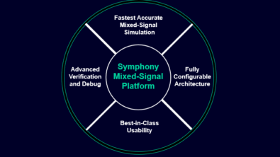
To learn more about Solido Custom IC solutions, click here.
To learn more about Samsung Foundry technologies, click here.