Manufacturing Intelligence: AI in the Fab
By Dr. Jim Shiely, Chief of Staff for Calibre Semiconductor R&D, Siemens EDA
With the rapid rise of AI, semiconductor manufacturing is entering a new phase—not just of incremental improvement, but of fundamentally different operating dynamics inside the fab.
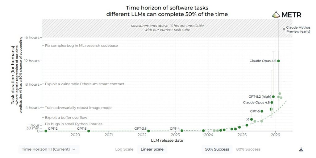
We often frame our industry’s progress in terms of Moore’s Law. That framing feels incomplete. What matters now is not just scaling devices—it’s the rate at which we can explore, validate and deploy new ideas. The industry is beginning to resemble a self-reinforcing acceleration loop. We are moving from Moore’s Law toward a more aggressive, compounding dynamic—closer to Kurzweil’s Law of Accelerating Returns. Figure 1 shows how rapidly AI models like LLMs are closing the gap to human performance, moving from simple to complex software tasks in hours instead of days, dramatically easing the developer bottleneck and accelerating the feedback loop.
AI tightens feedback loops
AI is not simply making individual tasks faster. It is tightening the feedback loops that govern how quickly we can iterate. As those loops compress, long-standing bottlenecks begin to fall away—and new ones emerge just as quickly. The result is not just a smoother system, but a faster one, where constraints continuously shift.
In IC manufacturing, bottlenecks have traditionally been easy to identify. They are tied to physical constraints such as equipment throughput, wafer processing capacity, logistics or tool and material availability. But constraints increasingly appear in less obvious places:
- Metrology stages, where measurement capacity limits learning
- Data pipelines, where petabytes of information must be refined into something actionable
- Decision processes, where interpreting results becomes the gating factor
In addition to production bottlenecks, innovation bottlenecks are just as critical:
- The time required to optimize processes
- The complexity of configuring software flows
- The challenge of co-optimizing device, process and mask
AI will knock down some of these bottlenecks. As some barriers fall—particularly those related to exploration, configuration and orchestration—new ones will become more visible. Increasingly, the limiting factor is not the ability to run experiments, but the ability to decide what results to trust and what actions to take next.
AI as an orchestrator, not a replacement
Much of the discussion around AI suggests that it will replace existing tools or workflows. In semiconductor manufacturing, a more accurate view is emerging. AI in the fab acts primarily as an orchestration layer. It coordinates the operation of:
- Physics-based simulation tools
- Data analysis pipelines
- Process control systems
- Engineering workflows
The underlying tools—like the Calibre software performing rigorous calculations, modeling physical behavior or processing wafer data—remain deterministic and highly validated. AI does not replace them. It makes them easier to use, more connected and far more productive.
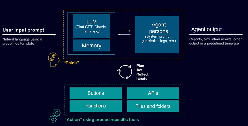
As a result, these tools tend to be used more, not less. As they become easier to operate and more efficient, engineers expand the scope of what they attempt. The net effect is not reduced demand for engineering tools, but increased reliance on them.
The emerging triad: simulation, metrology and intelligence
At the core of this transformation is a shift in how we think about data and experimentation inside the fab. A useful way to frame this is through a simple triad:
- Simulation defines the feasible search space
- Metrology constrains that space with real observations
- AI prioritizes where to act and orchestrates intervention
This triad effectively defines the operating model of the modern fab: exploration, grounding and intervention.
Simulation is no longer limited to lithography models. It is expanding to encompass broader manufacturing behavior:
- Process interactions across layers
- Equipment behavior and variability
- Even aspects of metrology itself
These simulation capabilities are becoming a foundational part of the digital twin infrastructure—not just describing the system but enabling engineers to explore it at scale.
Metrology, in turn, anchors everything in reality. No amount of simulation can replace the grounding that comes from actual wafer measurements. But measurement alone is not sufficient. It must be interpreted in context, connected back to models and used to update our understanding of the system.
AI operates between these two domains. It navigates across large design and process spaces, identifies promising interventions and coordinates how tools are used to validate them. Importantly, its influence extends beyond traditional areas like OPC. It begins to inform broader manufacturing decisions across the flow.
Acceleration exposes new challenges
As these capabilities combine, the rate of iteration increases. Engineers can explore more options, evaluate more scenarios and refine processes more quickly than before. But this acceleration comes with new challenges. When iteration cycles compress, the system becomes more sensitive to:
- Data quality and consistency
- Model fidelity and applicability
- Reproducibility of results
- Transparency of decision-making
In other words, the bottleneck shifts from execution to interpretation. The question is no longer just whether we can generate answers—but whether we can understand them well enough to trust them.
The future role of engineers
AI systems can orchestrate workflows and propose actions, but they do not replace the need for an engineer’s judgment. If anything, they increase its importance.
Engineers are increasingly responsible for:
- Understanding how results are produced
- Evaluating whether those results are meaningful
- Deciding how to act on them
The old rule still applies: show your work. But now, it is not just the engineer who must do so. The systems we build—especially those driven by AI—must also provide visibility into what they did, how they did it and why.
The path forward
The shift toward manufacturing intelligence is not defined by any single tool or capability. It emerges from the interaction between systems:
- Simulation expanding the space of what can be explored
- Metrology grounding that exploration in reality
- AI accelerating how we connect the two
Together, they create a system that moves faster than the one it replaces. The challenge goes beyond “keeping up with AI.” It is learning how to operate responsibly within an environment where the timescale of feedback loops is compressing and decisions must be made more quickly than before. The future of semiconductor manufacturing will be defined by how well we manage that balance—between speed and control, exploration and validation, automation and understanding.
The acceleration is already underway.
This blog touches on the topics I cover in a recent panel discussion, which is available on demand here.
For more on this topic, read our whitepaper AI and ML in Calibre IC Manufacturing: the intelligent solutions driving innovation