Siemens and UMC extend partnership to bolster the chip ecosystem

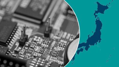
Chip demand is at an all-time high due to a multitude of factors. For starters, the unexpected global pandemic has affected throughput of foundry production significantly since 2020. Furthermore, chips are now being incorporated into pretty much all industries for technological advancements to enhance usability, features and customer experience – whether automotive, medical, industrial, communications, networking, computing or IoT. This technological renaissance has paved the way to the rapid emergence of countless silicon start-ups around the world. It has encouraged established IC makers to expand with newer silicon development teams. It has even enticed companies that historically purchase chips from others to now setup their own internal IC design shops. The global geo-political situation has further fueled the uncertainty of raw material availability for chip fabrication across geographic boundaries. Needless to say, semiconductor foundries have been feeling extreme pressure to navigate the current manufacturing roadblocks to first overcome backlog, and then to support the rapidly incoming new orders. They not only need to expand capacity but also need to continue innovating towards newer process technologies that deliver superior performance and reliability.
UMC (United Microelectronics Corporation) stands firmly in the elite group of semiconductor foundries committed to deliver quality technology. In fact, they are the first semiconductor foundry to commit to net zero emissions by 2050. Headquartered in Hsinchu, Taiwan, UMC is a pureplay foundry that provides high quality IC fabrication services, focusing on logic and various specialty technologies to support all major sectors of the electronics industry. Their IC processing technologies and manufacturing solutions include Logic/Mixed-Signal, embedded High-Voltage, embedded Non-Volatile-Memory, RFSOI and BCD etc. UMC has a total of 12 fabs in production with a combined capacity close to 800,000 wafers per month, that are certified with IATF-16949 automotive quality standard.
Having a leading edge fab house is important but if the IC developer is not able to design quickly and reliably to send a die foot print for fabrication with a timely tapeout, then what is the point. You need an EDA solution that supports front-end through back-end design, verification and debug. Knock Knock. Who’s there? Siemens EDA !
I have utilized many EDA tools from different providers in my prior design career. As a prior customer of Mentor (now part of Siemens), I always appreciated the tenacity with which the Analog and Mixed Signal (AMS) verification products constantly upped their quality and features. Those attributes are even more amplified now with the latest technological advancements of Analog FastSPICE (AFS) Platform. It’s high performance transient and RF circuit simulation engines with AFS eXTreme technology, mixed-signal verification and debug with Symphony, variation aware design capability with Solido Variation Designer, dynamic EMIR analysis with Calibre mPower and analog fault analysis with Tessent DefectSim provides a comprehensive recipe for an IC designer to efficiently design and verify leaf circuits, blocks, sub-systems and full blown IPs. High capacity, performance and accuracy has always been the AMS motto, and product enhancements continue to be done each quarter.
UMC and Siemens continue to advance their partnership with technology certifications through the difficult pandemic to enable mutual customers.
In March 2020, Siemens EDA’s Calibre platform and Analog FastSPICE platform were certified for UMC’s 22nm ultra-low-power process technology. UMC’s 22nm process platform is currently in volume production and includes both ultra-low power (ULP) and ultra-low leakage (ULL) options. The 22nm process platform offers silicon infrastructure for various semiconductor applications, including consumer electronics, digital TVs, monitors, and power or leakage sensitive IoT chips (with Bluetooth or Wi-Fi) that are ideal for wearables requiring extended battery life. Press release announcing this certification for UMC 22nm ULP process node >> Click Here
In March 2022, UMC’s 28HPC U+ process technology was AFS certified. UMC’s 28HPC U+ platform offers a good balance between cost considerations and chip performance, and is well-suited for a range of applications requiring high-speed and low-power consumption, including integrated circuits (ICs) for Wi-Fi, digital TV and flash controllers applications. Compared to UMC’s 28nm technology, the high-performance, low-power 28HPCU+ platform can offer up to a 15 percent boost in performance. Press release announcing AFS certification for UMC 28HPC U+ process technology >> Click Here.
More UMC technology qualifications are underway. Stay tuned!
To learn more about UMC certified Siemens EDA solutions, visit: Analog Mixed-Signal Verification and Calibre Design Solutions.
To learn more about UMC’s portfolio, visit: https://www.umc.com/en/home/Index