Solder strength testing and validation

Strengthening PCB Solder Connections

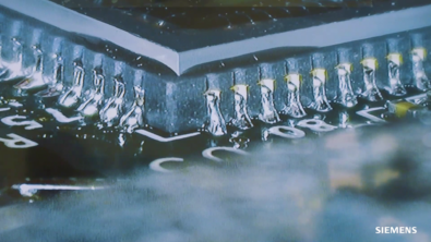
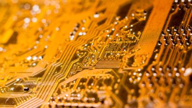
To increasing the overall solder strength within a PCB design, designers should be focusing on two distinct but related factors: The material composition of the solder, and the pad and footprint layouts for individual components. The composition of the solder itself will depend upon the application of the board, the components, construction method and materials within the board, and the overall final board quality. The overall footprint of the component will be dependent upon the components within a BOM and the recommended assembly guidelines of your assemblers. Both of these factors rely on discussions and interactions with your assembly house and leaving these discussions until after the design has been released ultimately limits your assembly options.

Exploring Manufacturing Driven Design for automated DFM

Manufacturing Driven Design leverages the intelligence within your PCB Design

Intelligent Process-Driven DFM Analysis for PCB Designers Recent component shortages and distribution disruptions have exposed both the fragility of global…

PCB Design and Stencil

Stencil design considerations during library cell design

Library cell design seems to be an easy part of the entire design process, but in reality, it can be a complicated part of this process, as it involves many different aspects to consider. It should not only comply with the electrical needs, but also needs to meet manufacturing requirements. Solder paste printing is one of the manufacturing processes that may need considerations during your library cell creation. To be more straightforward, the stencil design is something need to be considered during library cell design.

pick and place machine on PCB SMT line

How to Optimize PCB Design for the SMT Assembly Process Flow

PCB (Printed Circuit Board) design layout optimization is critical for the success of SMT (Surface Mount Technology) assembly. SMT assembly involves placing surface mount components directly onto the surface of the PCB, as opposed to through-hole components, which require holes to be drilled through the PCB. SMT assembly is faster, more precise, and more cost-effective than through-hole assembly, but it requires careful design optimization to ensure a successful assembly process.

Migrating from Gerber to ODB++ CAM Compare

Gerber files have long been the industry standard for PCB design and manufacturing data. However, with the increasing complexity of modern designs, Gerber files have become less effective in conveying all the necessary data required for manufacturing. ODB++ is a newer format that was developed specifically to address the shortcomings of Gerber files. ODB++ is a comprehensive format that includes all the necessary data for manufacturing, including component placement, drill files, and manufacturing details such as the thickness of the PCB and the type of solder mask just to mention a few.

Rigid-Flex Material Considerations

Flex and rigid-flex designs refer to a PCB that is partially or entirely constructed using flexible rather than exclusively rigid…

What’s New in Valor NPI 2305

Valor NPI has recently been updated with version 2305. Included within are many of the revisions and feature updates for this latest version of the software

new features for stackup planning

What’s New in Z-planner V2023.1

Z-planner V2023.1 builds on previous versions by enhancing rigid/flex useability, tighter integration with Xpedition and HyperLynx and the addition of more Mil-Aero materials to the dielectric materials library.

PCB Material Selection

6 material properties that can save you money when designing your PCB stackup

Introduction Stackup decisions are critical to every PCB and electronic product, but they don’t always get the attention that they…