You Need to Control Your PCB Stackups!

Stackups are critical to PCB Design
Stackups.
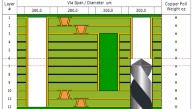
They are a critical part of any PCB design, even the simple double-sided board. At the bare minimum, the board layers have to deliver the required performance when fabricated. For many of you, you create the stackup and rely on the fabricator to provide your requested PCB stackup design and material choice.
But, there is a problem and it can completely derail your product: not all fabricators will produce the same exact board given the same output data. How can that be? Simple: each fabricator has their own proprietary work flow. That doesn’t create a problem for slower-speed signals, but for boards operating with clock speeds in the GHz range, it’s a different ballgame.
Let’s say you send your data to two different fabricators. They produce your boards to your specification. Upon incoming test, however, one works perfectly and the other won’t work at all. Solving this generally requires more interaction with your fabricator than conventional lower-speed boards, and possibly more than one iteration.
Simulation to verify PCB functionality
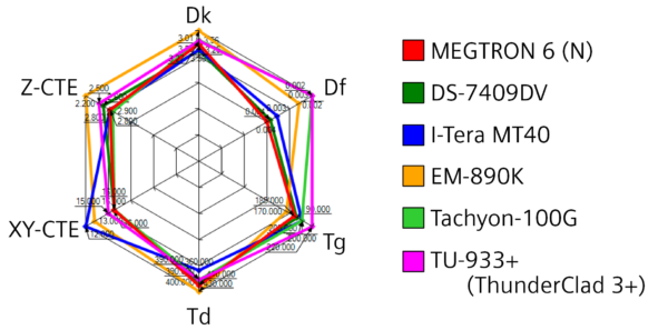
In many cases, simulation is used to virtually verify PCB functionality. Unfortunately, many engineers simulate without knowing exact dielectric thicknesses, Dks, and Dfs as a function of resin content and frequency. While the board may look fine in the simulation, actual use of the materials can be different.
The logical approach to producing high-speed boards would be to bring extensive knowledge of fabrication, including intimate knowledge of the properties of the materials used for the board. Unfortunately, someone with that kind of knowledge is an expensive hire, and unless you are designing high-speed boards frequently, that person may not be needed for every design.
Now, however, the new Z-planner Enterprise software from Valor brings the expert fabrication knowledge to your products at a fraction of what it would cost to employ a fulltime expert. Z-planner Enterprise aids you in both selection of material and construction of the PCB stackup design, and also allows you to manage the stackup instead of the fabricator. Recently, Bill Hargin, lead Engineer at Z-planner Enterprise, released a detailed e-book on stackup which digs deep into the factors involved with stackup planning.
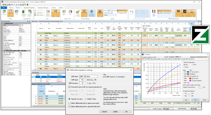
Z-planner Enterprise contains all the tools you need to design and verify stackups on fast PCB designs. In addition to being able to calculate impedance and design valid stackups, you can run the field solver and perform cross-section analysis. And, it includes the industry’s largest dielectric materials library, including laminates. The result is a stackup design that will produce first-time-right results regardless of the fabricator. Sound interesting? It is! You can take a deeper look at Z-Planner Enterprise on their website, or download the free trial today.