Printed circuit board design process goes digital for reliability – part 2 of 8
Many engineering organizations want proof that a printed circuit board design process will meet the next generation requirements. What does that mean?
Traditionally, this was done through testing in thermal chambers and vibration cells with many hours of testing, resulting in a certain number of units with a specified limit of failures. However, parts would often not pass, and this would require a redesign or new components – resulting in cost overruns and missed deadlines.
Currently, companies want proof early in the printed circuit board design process to verify that you know what you’re doing: this means using digitalization and simulation. Traditionally, simulation would account for circuit simulation for functionality, circuit board trace layout and maybe some basic level of thermal analysis. This is no longer sufficient to demonstrate that a circuit board design proposal will meet safety critical requirements.
Next generation simulation technologies that account for functional performance from end-to-end meet this need. Current simulation processes are disjointed, disconnected and not flexible. This is further exacerbated by the fact that different engineering domains were involved: electrical and mechanical. What’s needed is an integrated printed circuit board design process that could quickly evaluate all relevant physics of a circuit board design forward and backward.
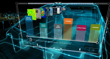
Essentially, all aspects of performance are evaluated. This includes:
• Circuit performance
• Layout optimization
• Static and transient power dissipation
• Conjugate thermal analysis (airflow, conduction, and radiation)
• Structural stress (vibration & thermal), and
• Fatigue down to the solder joint level.
Often, it can be a small crack in a solder joint, plated hole or leaded component that can cause substantial degradation in performance. These all need to be evaluated in consideration as a part of the printed circuit board design process.
For example, a high current trace may run underneath a controller chip, which amplifies the operation temperature and can reduce durability and operational life. But, moving the chip to another location can result in other unanticipated problems due to vibration, voltage drop and thermal stress.
An integrated simulation process allows for timely assessment of such changes to ensure the performance targets are all achieved.
This is where digitalization comes into play. All aspects of the printed circuit board design process need to be simulated and evaluated to ensure safety and reliability are achieved. As many different engineering activities interact with this development, a full end-to-end development process and simulation are required to ensure all efforts work together harmoniously to achieve functional, timing and costs targets.
This concludes the second part of our series on electronics systems and the challenges to provide solutions for products of the future. In part three, we’ll continue discussing electronic systems and the circuit board development process. If you wish to start from part 1, please click here.
About the author
Greg Roth is the director of automotive and transportation solutions in the Industries Group at Siemens PLM Software. In his current role, he champions CAD, CAE & PLM technologies and processes for companies at a global enterprise level so they can achieve substantial reductions in product development costs and time while improving overall quality. He previously held positions at Ford Motor Company, Eaton Corporation and Amcor Packaging. He was also chief engineer for the CAE and NVH departments at ZF-TRW Automotive North America Braking Systems in Livonia, Michigan. Greg holds an master’s degree in mechanical engineering from the University of Michigan, a master’s degree in electronics and computer controls engineering from Wayne State University and a bachelor’s degree in mechanical engineering from Michigan State University.