3D IC Test: Now and the Road Ahead
By Martin Keim, Mentor Graphics
What’s new in 3D IC testing? This summary from an ISTFA tutorial has the answers
Solutions for 3D IC test are ready today, but they will be more ready tomorrow. At the 2015 ISTFA, I presented a tutorial titled “What is New in 3D, Digital Testing?” and I’ll summarize the main points here. I consider test standards and test challenges, which include known-good-die and testing stacked die.
The two main goals of 3D IC test are to improve the pre-packaged test quality and to establish new tests between the stacked die. Of course, high-quality test in 2D (known-good-die) is a basic prerequisite to testing 3D stacks. The problems are well understood and good solutions exist. There are some solutions for testing memory stacked on logic and memory stacked on memory. However, 3D test for logic-on-logic stacks is still in its infancy. To address a range of 3D testing needs, the industry has been actively working to finalize or update several existing test standards, including:
- IEEE 1149.1 (JTAG), the well-known test access standard
- IEEE 1687 (IJTAG), the newer IP access methodology
- IEEE P1838, the proposed standard for 3D interoperability between multiple die and interfacing with other standards
- JEDEC standards, like JESD226 for wide-IO memory test
What 3D means for die-level test quality
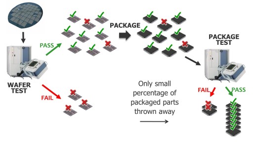
Before 3D testing, the wafer went through wafer test; some die passed, some failed. The good die went on to packaging, then packaging test, where a few more (escaped) failures would be found (Figure 1).
Figure 1: Traditional wafer vs package test. Some bad die escape tests, get thrown away. No biggie.
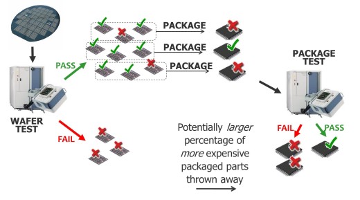
No big deal in the scheme of things. However, once you start packaging multiple die together, those few escapes from die-level test mean you are throwing out more packaged parts (Figure 2).
Figure 2: Wafer vs package test with 3D ICs. When escaped bad parts end up in multi-chip packages, the losses can be significant.
This is a very big deal. I ran some numbers: if your die defect coverage is 95%, the final package yield for a 10-die stack would be something like 60%. Clearly, a 5% escape rate is not good enough if it leads to 40% of your final product being tossed in the rubbish bin. The point is that 3D packages require very high-quality die-level test, so that only “known-good-die” (KGD) are packaged together.
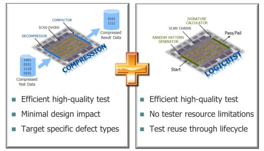
In addition to a high KGD requirement, 3D testing also calls for known-good-interposers, partial stack testing, testing through-silicon vias (TSVs), and die test in-package. Traditional ATPG alone is a thing of the past. A combination of embedded compression and logic BIST delivers the best quality vs. cost (Fig 3).
Figure 3: A hybrid test methodology includes embedded compression (ATPG) plus logic BIST. The two share test logic and offer a number of benefits.
The logic BIST part allows for in-system test that is particularly important to ICs for automotive or medical applications. Adding cell-internal and non-traditional fault models should bring the quality to acceptable levels for the digital logic part of the design. Of course, you also need to test embedded IP and the I/Os and TSVs. To access and test embedded IP, IEEE 1687 IJTAG provides an IP and pattern reuse methodology for integrating heterogenous IP. There are even tools that automate many of design and test tasks to enable the IJTAG methodology.
For I/Os and TSVs, testing must be done ‘contact-less’ because electrical contact to the ATE is not guaranteed. This is an area of active research to watch, one interesting idea is to use a boundary scan-type approach to enable test at the die-level of the partially packaged device, and of the interconnect between the dies in the package.
How to get test access through stacked die
Testing 3D ICs means accessing each die in the stack through a single point. Dedicated TSVs are used for test signals between die and each die has control hardware to route the test date up and down the stack. To make this a reality, we need a standard architecture to support heterogonous die from multiple vendors. The IEEE P1838 standard under development promises to do just that. Although by design, an 1838-compliant die would not be ‘plug-and-play’ because the standard addresses the DFT architecture only, but not the footprint, mechanical, and electrical interconnect properties.
Test External DRAM or Stacked Memory
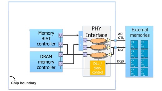
The most common use of 3D and 2.5D packages today is for external memories stacked on logic die or on the interposer, next to a logic die. The memories are usually DRAMs (although other memory types seem to get some tracking now) that follow a standard protocol. We developed a test interface to access external Wide IO DRAMs through their JEDEC standard functional pins. The 3D IC memory BIST includes the physical interface logic (PHY), and is located within the logic die, next to the memory controller and right before the PHY and its associated external memory (Figure 4).
Figure 4: Mentor’s test interface accesses external Wide IO DRAMs so you can swap memories from different vendors.
An advantage of using external memories in a package is that memories from different vendors can be swapped for cost or quality reasons (a.k.a. “second-sourcing”). The second-source die should still perform fine in the 3D package if it follows the same standard, such as Wide I/O. The memory pinout and operation will need to remain the same across different vendors. However, the internal physical layout of memory cells could vary. In those cases, you can use a pseudo-random data algorithm during memory BIST test that detects neighborhood pattern-sensitive faults (NPSFs) when the physical layout of the memory is unknown. You can load new algorithms into the soft-programmable memory BIST controller in case more targeted tests become necessary; there is no need to modify the design.
The takeaway is that 3D test challenges are well understood, and there are readily available solutions for most 3D IC test requirements. The foundation of 3D IC test is very high-quality die-level test. We still need logic-to-logic test solutions and the main challenge with that is synchronizing events during die-to-die at-speed testing. The completion of IEEE P1838 should be a big help. Testing memory in 3D or 2.5D is very much like testing external DRAM or WideIO memories. We also might need to test the interposers. Interposer test is an entire topic that deserves its own blog, so I’ll just quickly walk away from the topic and save it for another day.
Liked this article? Then try this –
White Paper: Plug-and-Play Test Strategy for 3D ICs
This article was originally published on www.3dincites.com

