Why Not Just Shove a Heatsink on Top of it? Part 3: Pads, Vias and Undersinking
An appreciation of heat flow paths is a pre-requisite for good thermal design. If you attempt to augment heat flow where there is none then your expectations are as futile as your design skills. The real value of simulation for me is that it enables an insight into the behaviour of a proposed design (this is true for simulation of any design and any behaviour). Once you understand the true physics of the behaviour you can then have the power to make specific enhancements with a high probability of success. With that in mind it is a little disheartening to see so much simulation using FloTHERM conducted simply to find out ‘if my electronics will get too hot’. Thermal verification has its place but that place should be behind the application of simulation for thermal design (or after, if you want to be chronologically pedantic).
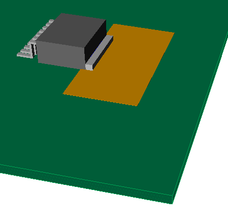 Knowing that for the TO package the majority of the heat flow is going down into the PCB, regardless of whether a heatsink is plonked on top of it, let’s see if we can augment that heat flow by reducing the thermal resistance of the board. This can be done in two parts. Having the tab of the package sit on a large copper pad will spread the heat away from the package to a larger area of the board. Then, adding an array of through hole vias (for thermal purposes) under that pad will help get the heat to the spreading metallic planes within the board.
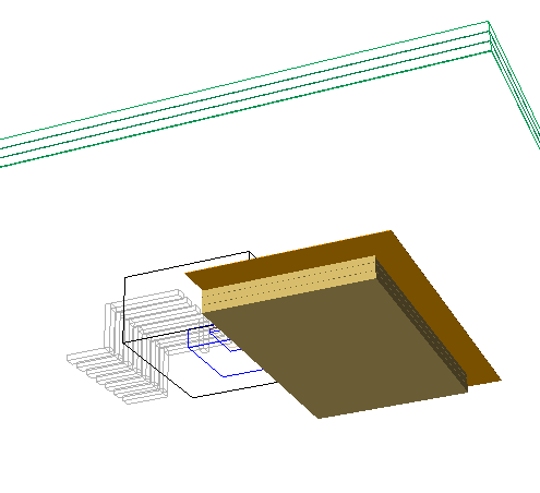 From a simulation perspective I’ve modelled the array of vias as a volume of the board with modified in plane and through plane thermal conductivity values, calculated from knowledge of the Cu/FR4 distribution within that volume. The key being that the thermal effect of the vias is to punch through the FR4, taking the through plane conductivity from 0.3 W/mK up to over 6 W/mK (depending on the number of vias in that area). Much simpler to define and solve, though sure, model the individual vias if you want. Good to know you have enough time to do that, does your boss know that as well?
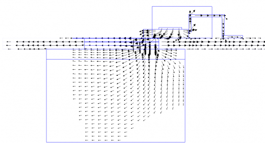
The result is that the temperature rise of the junction over ambient halves. Not bad. The additional spreading of the heat inside the PCB can be seen by looking at the heat flux vectors. You can see the heat bursting through the dielectric layers and spreading in the metallic layers. That get the heat to a wider surface are of the board, both on top and bottom faces, where the air can then whisk it away.
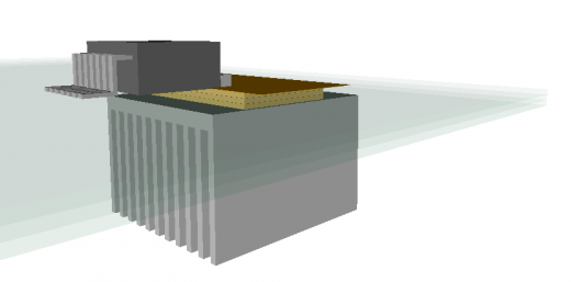
Why not go one step further? Now that the heat’s getting to the underside of the PCB let’s augment that heat flow path even more by putting our original heatsink on the underside of the board and see what happens?
The result is a further halving of the temperature rise. The use of simulation at the conceptual or architectural phase of a design process can lead to such radical improvements in the design. Later on in the process it’s much more difficult, even squeezing a few % extra drop out can be extremely difficult. The whole design has been detailed down, removing wriggle room and leaving simulation good for no more than our friend verification (“is it too hot?”). 
A simulation based approach to obtain insights into design and design variants can save you time and money in finding a cost effective thermal solution. Without it there would have been the risk in this study of employing a very big, expensive and badly placed heatsink. As I’m sure must have been said by wife to husband a number of times: “it’s not what you’ve got, it’s how you use it that matters”.
5th July 2013, Ross-on-Wye.

