Bridging the gap between design and manufacturing in semiconductor production
The semiconductor industry is entering a new phase of innovation, pushing the limits of what is physically possible. Yet alongside these advances, a familiar challenge continues to surface: the disconnect between design intent and manufacturing reality.
It is no longer only a question of physics or scaling. Increasingly, the challenge lies in how information moves, or fails to move, between engineering and the fab.
This gap, often hidden behind highly automated processes, continues to impact yield, timelines and overall efficiency. Addressing it requires more than incremental improvements. It calls for a more connected approach to how data, intent and execution come together across the lifecycle.
The complexity wall and the data handover dilemma
Semiconductor manufacturing has always been complex, but that complexity is now reaching a new level. With inverted Bills of Materials (BOMs) and a constant interaction between process and discrete manufacturing, even small inconsistencies can have outsized effects.
As fabs become more automated and data-rich, the handover from design to manufacturing has quietly become an important source of yield loss. And not only for leading-edge nodes, this is just as visible in mature environments.
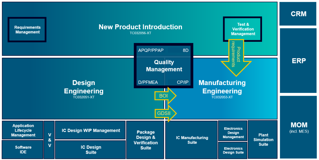
Traditionally, product engineers working in Semiconductor Lifecycle Management (SLcM) systems define the “what”: product requirements, design artifacts and GDSII files. In parallel, fab teams working in Manufacturing Execution Systems (MES) focus on the “how”: recipes, routing and equipment configurations.
Both perspectives are essential. But the connection between them is often less structured than expected.
In practice, this exchange still relies heavily on manual interpretation and disconnected data sets. SLcM contains rich design context, but has limited visibility into equipment constraints. MES controls execution in detail, but lacks the full background of why a process is defined the way it is.
The result is a persistent data gap, one that slows down new product introduction, introduces risk, and makes it harder to respond quickly to change. Across the industry, many solutions attempt to bridge this gap, but often through fragmented integrations that only partially address the root cause.
Moving toward a unified digital thread
At Siemens DISW, the focus is not just on connecting systems, but on aligning how information is structured and used across domains. The objective is to create a consistent, end-to-end digital thread that links design intent directly to manufacturing execution.
This is built on three tightly connected elements:
- the Bill of Information (BOI)
- the Bill of Process (BOP)
- the Bill of Equipment (BOE)
Each plays a distinct role, but their real value comes from how they work together.
The Bill of Information: establishing a reliable foundation
The BOI serves as the backbone of the product definition. Rather than acting as a static container, it captures the full scope of design intent, from EDA artifacts and die-level information to test programs and defect models.
Every element is versioned, governed and traceable. This creates a clear and controlled view of what the product is, how it evolves, and which data is valid at any point in time.
More importantly, it removes ambiguity. Manufacturing no longer starts from a partial or interpreted dataset, but from a structured and trusted source.
The Bill of Process: translating design into manufacturing logic
Once a design is released, the challenge shifts to making it producible.
The Bill of process provides that bridge. It takes the product definition and translates it into a structured manufacturing flow, covering all required steps, from front-end fabrication through test and assembly.
Instead of manually recreating data inside the MES, engineers take the existing definition as a starting point and enrich it with manufacturing information. The process is refined and contextualized, not re-entered.
This reduces the effort involved, but also the variability. Built-in best practices, standardized flows and controlled revisions help ensure that what is planned remains consistent with what was designed.
The inspection definitions coming from the quality planning are seamlessly integrated with the BOP, thereby incorporating the quality aspects as an integral element of the design intent.
The MES then takes this validated process definition further, adding the operational detail needed for execution on the shop floor.
The Bill of Equipment (BOE): aligning process with capability
A process is only meaningful if it can be executed with the available resources.
The Bill of equipment closes that loop by linking each process step to the actual equipment and capabilities within the fab. It creates a three-way alignment between design, processes and resources.
This step is often underestimated, but it plays a crucial role. Validating process plans against real factory constraints early on helps avoiding late-stage adjustments, eliminating production delays and unnecessary iterations.
From digital thread to factory floor reality
When these elements are connected, the transition to execution becomes much more straightforward.
Process definitions can be transferred directly to the MES environment, where they drive routing, instructions and machine configurations. For operators on the floor, this reduces uncertainty. There is less reliance on interpretation, and more confidence that the right version of the process is being executed.
Traceability is built in from the start. Every die produced carries a complete genealogy, linking back to the lot, the process definition and ultimately the original design. This makes it easier to investigate issues, validate quality, and support continuous improvement.
Strategic benefits and the future of semiconductor manufacturing
By connecting the BOI, BOP, and BOE, Siemens Software isn’t just managing data; they are automating the entire nervous system of the fab. This integrated approach delivers significant strategic benefits:
- Reduced yield loss: By closing the data gap between design and manufacturing, we minimize errors and inconsistencies, leading to higher yields and reduced scrap.
- Accelerated time-to-market: Automated data flow and validation streamline the entire process, enabling faster product introduction and quicker ramp-up to production.
- Enhanced IP security: With geopolitical tensions rising, securing IP from design to wafer fabrication is critical. The SLcM-MES bridge ensures IP is encrypted and version-controlled throughout the thread.
- Improved quality and compliance: The unified digital thread ensures consistent execution, facilitating compliance with stringent industry regulations and maintaining high-quality standards.
- Greater agility and resilience: The ability to rapidly adapt to design changes and manufacturing variations provides unprecedented agility and resilience in a dynamic market.
- Optimized resource utilization: By understanding equipment capabilities and process requirements, fabs can optimize resource allocation and improve operational efficiency.
Looking ahead
The semiconductor industry will continue to increase in complexity. More steps, more variants, more dependencies between domains.
In that context, simply adding more tools or more data will not be enough. What matters is how that information is connected and how reliably intent is carried from design to execution.
By creating a structured, end-to-end approach that links product definition, process planning and factory capability, Siemens Software is helping semiconductor manufacturers reduce friction where it matters most.
The result is a more consistent path from concept to production, one where design intent is preserved, execution is aligned, and outcomes become more predictable as complexity grows.
Learn more at siemens.com/opcenter-semi