5 Expert Articles from EDA and Beyond
- Correlating Software Execution with Switching Activity to Save Power in SoC Designs
- Searching for Extraterrestrials
- Reducing PCB Failure Rates Due to Vibration and Acceleration
- How Critical Area Analysis Optimizes Memory Redundancy Design
- Betting On Wafer-Level Fan-Outs
Correlating Software Execution with Switching Activity to Save Power in SoC Designs
Semiconductor Engineering
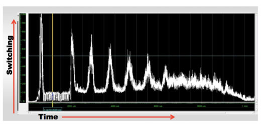 To save power in SoC designs without compromising functionality, system developers are adding the ability to turn off the parts of the system that are not being used. Most of the time, the power saving system works well. But occasionally, the battery dies much sooner than it should. This article explains how emulation and Codelink debugged this elusive low-power problem in an ARM multiprocessor design.
Searching for Extraterrestrials
SemiWiki
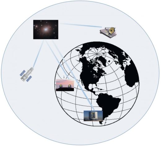 Analog-to-digital converters (ADC) play a key role in space and ground telescopes. The ADC must meet exacting demands in differential linearity and dynamic range in order to be suitable for ground-based telescopes. Add to that low power demands (<1.5mW) for space telescope use and you have almost impossible requirements. This article discusses designing ADC converters using the Tanner AMS design flow.
Reducing PCB Failure Rates Due to Vibration and Acceleration
ECN Magazine
 PCB designers can avoid premature product failure by adding virtual vibration and acceleration simulation during layout. This enables design teams to improve design quality, while shaving off weeks, or even months, of costly physical failure analysis.
How Critical Area Analysis Optimizes Memory Redundancy Design
SemiMD
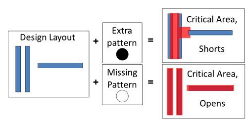 Critical area analysis (CAA) can tell you if your redundant memory elements are actually useful, or a waste of time and money. Since most large SoC embedded memories often cover 40-60% of the chip area, that’s valuable information for improving yield while managing design and manufacturing costs. This in-depth article covers all of the details relating to CAA and optimizing memory redundancy design.
Betting On Wafer-Level Fan-Outs
Semiconductor Engineering
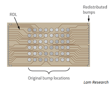 To reduce routing issues at 10nm/7nm, chipmakers are focusing on fan-out wafer level packaging (FOWLP). This requires new and unique tool flows and design methodologies. Experts discuss how EDA companies are busy developing solutions to that enable companies to spend more time up front virtually to determine how to construct multiple die inside a package before they commit to a physical detailed design.
Comments
Leave a Reply
You must be logged in to post a comment.
Great