Article Roundup: EDA & IP Growth, HLS SLEC, Model-Based Hinting at Sub-20nm, an Integrated PCB Verification Platform & Software approaches to Hardware Verification
- EDA, IP Show Strong Growth
- Sequential Equivalency Checks in HLS
- Enhanced model-based hinting may be the edge you need below 20nm
- Eliminate PCB Re Spins using an Integrated Multi Dimensional Verification Platform
- Using Software Approaches In Hardware Verification
EDA, IP Show Strong Growth
SemiEngineering
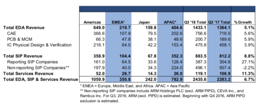 Worldwide EDA and IP revenue was up 6.7% in the third quarter of 2018, reaching $2.44 billion. This growth was fueled by increased investment in AI and 5G startups, along with the hoard of companies entering the automotive electrification and autonomy race. With abundant funding, there are many new fabless startups looking to buy design tools, providing a strong outlook for EDA.
Sequential Equivalency Checks in HLS
SemiWiki
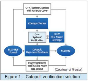 More companies are turning to HLS because of the availability of verification solutions that can validate generated RTL against the high-level C++ or SystemC. A key piece of these verification solutions is the equivalency checker. Sequential logic equivalency checkers (SLEC) provide formal validation across design abstractions and refinement stages to deliver more comprehensive verification with less effort.
Enhanced model-based hinting may be the edge you need below 20nm
Tech Design Forum
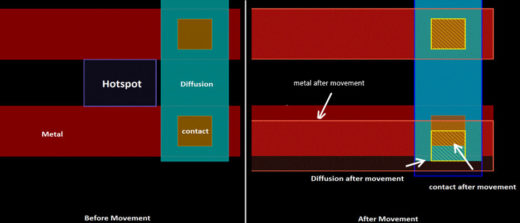 Resolving lithographic hotspots without unintentionally introducing new ones is challenging. To help, model-based hinting (MBH) solutions were added to lithographic checking tools, providing possible hotspot fixes that will not create new issues. For sub-20nm layouts with double-patterning, MBH has been extended to include multiple-layer DRC and rules for different masks to improve the accuracy of the hints.
Eliminate PCB Re Spins using an Integrated Multi Dimensional Verification Platform
SemiWiki
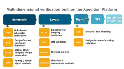 PCB design complexity is increasing along with mounting pressure to deliver state-of-the-art products to market as quickly as possible. Detecting and resolving potential issues early in the design flow is critical to meeting these demands as it prevents delays and expensive re-spins. A new multi-dimensional verification platform moves verification up in the design process and automates analysis to catch errors before they become problems.
Using Software Approaches In Hardware Verification
SemiEngineering
Hardware development teams are looking to adopt Agile methods to reduce the number of bugs in hardware designs. Agile, however, was initially conceptualized for software development, meaning the concepts do not translate perfectly to hardware. This article examines how hardware teams are adapting Agile methods to improve their development processes.