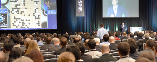
Mentor at SPIE Advanced Lithography 2018
SPIE Advanced Lithography, the premier conference for the lithography community, will be held at the San Jose Convention Center February 25 – March 1, 2018. Mentor experts will be delivering conference papers, post sessions, and answering your questions in booth 222.

In the conference program, Mentor is showcasing two technological features – EUV readiness and our new OPC approach for handling memory applications & flows. Papers relevant to those focus areas are listed below:
EUV Readiness
- SRAF requirements, relevance, and impact on EUV lithography for next-generation beyond 7nm node
- Model-based hyper-NA anamorphic EUV OPC
- Impact of aberrations in EUV lithography: metal to via edge placement control
A new OPC approach for handling Memory applications & flows
- Model-based cell-array OPC for productivity improvement in memory fabrication
- Model-assisted template extraction application to contact hole patterns in high-end flash memory device fabrication
ALL CONFERENCE SESSIONS AND TIMES
SRAF requirements, relevance, and impact on EUV lithography for next-generation beyond 7nm node
Tuesday, February 26 | 1:30pm
Model-based hyper-NA anamorphic EUV OPC
Tuesday, February 26 | 2:10pm
Impact of aberrations in EUV lithography: metal to via edge placement control
Tuesday, February 26 | 2:30pm
A novel method to fast fix the post OPC weak-points through Calibre eqDRC application
Wednesday, February 28 | 8:45am
Constraint approaches for some inverse lithography problems with pixel-based mask
Wednesday, February 28 | 9:10am
Model-based cell-array OPC for productivity improvement in memory fabrication
Wednesday, February 28 | 10:30am
Model-assisted template extraction application to contact hole patterns in high-end flash memory device fabrication
Wednesday, February 28 | 11:10am
A model-based approach for the scattering-bar printing avoidance
Wednesday, February 28 | 2:30pm
A novel processing platform for post tape out flows
Wednesday, February 28 | 2:50pm
Combinational optical rule check on hotspot detection
Thursday, March 1 | 11:30am
Integrated manufacturing flow for selective-etching SADP/SAQP
Thursday, March 1 | 2:20pm
Comparison between traditional SADP/SAQP and selective-etching SADP/SAQP
Thursday, March 1 | 2:45pm
POSTER SESSIONS
Tuesday, February 27 | 5:30-7:30pm
Exploring EUV and SAQP pattering schemes at 5nm technology node
Ultimate patterning limits for EUV at 5nm node and beyond
Inverse lithography recipe optimization using genetic algorithm
Cross-MEEF assisted SRAF print avoidance approach
A weak pattern random creation method for lithography process tuning
A smart way to extract repeated structures of a layout
Using pattern-based layout comparison for a quick analysis of design changes
An efficient way of layout processing based on Calibre DRC and pattern matching for defects inspection application
Leverage Calibre pattern matching to address SRAM verification challenges at advanced nodes
EXHIBIT FLOOR
Visit Mentor experts in booth 222 to learn about our best-in-class technology, comprehensive solutions, development and production support, and continuous innovation. The challenges of developing advanced lithography flows require a strong partner. With a complete design-to-manufacturing platform for Immersion Lithography, EUV and DSA, Mentor, a Siemens Business, is the ideal partner for semiconductor manufacturing success.