Collaborative semiconductor business platform: the future of industry partnerships | Executive strategy deep-dive- Part 2
In this second installment of our interview series, we continue exploring Siemens’ three-pillar strategy for semiconductor industry transformation. Host Gabriella Leone sits down with Michael Munsey, Vice President of Semiconductors and Electronics at Siemens Digital Industries Software, to dive deeper into the first pillar’s technical capabilities and examine how collaborative business platforms are reshaping industry partnerships from project management to cross-domain optimization.
Next-generation capabilities for rapid industry changes
Q: Looking ahead, how do you see the collaborative semiconductor business platform evolving over the next 5 to 10 years? What new capabilities or features do you think will be essential to keep up with the industry’s rapid changes?
A: If you look at how semiconductor companies have traditionally tracked development efforts, scheduling, and interactions with manufacturing or OSATs, most business decisions have been done through manual efforts. I often joke that Excel is a great competitor to every product in every industry – many companies still use spreadsheets to track their projects.
This has kind of worked in the past, but when you rely on humans to input data into spreadsheets, there’s always the chance of error. Plus, by the time data goes into spreadsheets and gets rolled up, it tends to be a couple days old.
This is becoming an issue as semiconductor projects become more complex due to their size, cost, and the fact that companies are looking to collaborate with others to share development costs and burdens. What you need going forward is automation that mines the wealth of information produced by design and verification tools to actually track schedules and progress automatically.
The biggest change will be AI platforms built on top of all this information that not only extract things automatically, but start making inferences based on historical information. Is there a problem we’re not aware of that could put us behind schedule? Are we making decisions now that will affect downstream processes like functional verification, design closure, or manufacturing?
Siemens’ comprehensive cross-domain advantage
Q: Siemens is uniquely positioned to deliver a comprehensive solution that integrates software, semiconductor design, PCB design, and MCAD. How does this give Siemens an edge in enabling the collaborative platform?
A: When I was a semiconductor designer, my world was just the semiconductor. But semiconductors don’t exist independently – they’re part of products and solutions. Software runs on semiconductors, chips go on boards, boards get wired with harnesses, and they all get put into products designed from a manufacturing perspective.
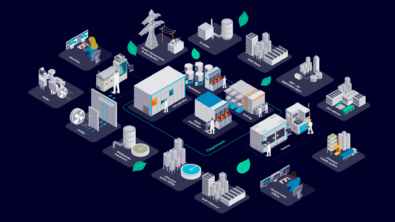
This is Siemens’ advantage: we understand all domains of product development. Whether it’s a mobile phone or automobile, you’re talking about convergence of software, semiconductors, ECAD systems, EE systems, and mechanical systems.
Starting from the NPI flow with the right requirements driving architecture, we can’t think about architecture just in terms of semiconductors – we need to think about the whole system. That means optimizing the system early and driving that into software development, semiconductor development, PCB development, wire harnesses, and the entire product.
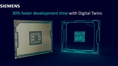
We bring a comprehensive digital twin that allows everything to be done and optimized in a virtual world first, getting requirements straight and driving all domains from an optimized set of requirements.
Lessons from industry challenges and partnerships
Q: In our first discussion, you talked about challenges companies like Intel are facing with project timelines and resource allocation. How do our platforms address these challenges and what lessons can other companies learn?
A: Most customers I talk to are collaborating with other companies. Look at Analog Devices’ recent MOU with Tata Electronics. Analog Devices has their own foundries, but for advanced node design and the cost of building new fabs, they’re partnering with Tata Electronics who are building fabs in India through Indian government investment.
But it goes further – Tata Motors needs an ECU supplier for their automobiles, and they’re looking to Analog Devices’ automotive division. So now you have cross-industry collaboration where Analog Devices operates both as an IDM and fabless company, working closely with Tata Electronics on manufacturing while collaborating with Tata Motors on automotive requirements.
This requires sharing requirements, aligning architectures and schedules, ensuring timely delivery, and providing virtual models for software development. You’re taking a complex system, spreading it across multiple companies, and still managing schedules and information sharing while ensuring both companies can move forward during development.
AI-driven automation and intelligence platforms
Q: What’s your one call to action to the semiconductor industry regarding collaboration?
A: Digitalization. The semiconductor industry was one of the leaders in developing digital twins because semiconductor design has to be done virtually – you never see the product until it comes out of manufacturing. But it’s not just the development process – it’s about digitizing your entire flow.
Understanding the NPI process, making sure project scheduling and requirements are tracked in systems open to digitalization, because then the collaboration platform can start linking all this data together. Taking real-time data from design and manufacturing, linking verification data back to requirements, having the thread that connects requirements through design, verification, integration, and testing.
Use that as proof points to sign off schedules and understand potential problems. It’s extending what the industry has done well for a long time across the entire ecosystem.
Overcoming barriers to information sharing
Q: What do you see as the biggest challenge in implementing the collaborative platform and how is Siemens working to overcome them?
A: Companies will have to open up information that’s been kept very close in the past. There’s certain design and development information held close to designers, manufacturing process information held close to fabs, and semiconductor equipment manufacturer IP held close to equipment makers.
But to keep up with the rate of change, fabs want to understand the designs they’re getting to ensure manufacturability and agreed-upon ramp rates. In the past, fabs did this by running test wafers over 6-9 months at large cost, tweaking processes in real time. But with newer technologies where wafer development time is 3-5 months, that ramp time is too long.
They need to do more virtually, requiring semiconductor equipment manufacturers to deliver digital twins of their equipment for virtual manufacturing modeling. There needs to be cooperation and information sharing that hasn’t existed before, with platforms that protect intellectual property while allowing the right information sharing.
What’s next?
Q: How does the first pillar tie into the other two pillars of your strategy?
A: Pillar 2 is about software-defined products. When software and semiconductor teams work together, you need the collaborative platform for these teams to optimize architectures upfront with the right requirements and development processes.
Software-defined products involve software, semiconductors, PCB design, EE systems, and mechanical aspects all working together – again, collaboration is key.
Pillar 3 is the digital twin from design to manufacturing. This is about design collaborating with manufacturing – ramping process nodes virtually, ramping new product designs in fabs virtually, taking real-time manufacturing information back into design libraries to optimize for better manufacturing ramps.
The next two pillars all build on the strong collaborative platform foundation.
The semiconductor industry is accelerating rapidly – from planar transistors lasting 50 years to FinFETs lasting 15 years to gate-all-around architectures lasting 5-10 years to CFETs on the horizon. This acceleration demands collaborative platforms as enabling technology to operate in an increasingly fast-moving industry.
Stay tuned for part three of our interview with Michael Munsey, where we will explore Pillar 2 and dive deeper into software-defined products and how they’re reshaping semiconductor development methodologies and business models.
Frequently asked questions
What is a collaborative semiconductor business platform?
A collaborative semiconductor business platform is a digital infrastructure that enables companies across the semiconductor ecosystem to share data, coordinate development efforts, and work together on complex projects while maintaining IP security. It replaces manual processes like spreadsheets with automated data mining and AI-driven insights.
How does collaboration help reduce semiconductor development costs?
Collaboration allows companies to share the enormous costs of advanced node design and fab construction. For example, partnerships like Analog Devices with Tata Electronics enable cost-sharing for manufacturing while accessing new markets and capabilities across different industries.
What role does AI play in semiconductor collaboration platforms?
AI platforms built on collaborative data can automatically extract insights from design and verification tools, predict potential problems before they occur, identify resource constraints, and make inferences about project timelines based on historical information.
How do companies protect IP while collaborating more openly?
Collaborative platforms include security protocols that allow selective sharing of the right information while protecting sensitive IP. Companies can share manufacturing data, schedule information, and requirements without exposing core design secrets or proprietary processes.
What industries benefit from semiconductor collaboration platforms?
Any industry using semiconductors benefits, including automotive (software-defined vehicles), mobile devices, data centers, industrial equipment, and emerging AI applications. Cross-industry partnerships are becoming increasingly common as technology convergence accelerates.