ABCs of PCBs – H for Hierarchy
Welcome to ABCs of PCBs – a blog series to help new engineers learn about the world of Printed Circuit Boards. I’ll be covering topics from general engineering concepts to PCB design specific rules. As this is a ‘basics’ blog, I’ll keep the content software independent, but any visuals will be from the Mentor PADS Professional PCB suite.
If you missed the last post in this series: ABCs of PCBs – G for Ground Planes click here!
Just like hierarchy in universities (Dean > Director of Engineering > Professor > Teachers’ Assistant > Students), hierarchy in PCB design can help keep things organized and efficient. In the PCB schematic world, hierarchical design is a practice in which functional groupings of a design are represented by block symbols. You may hear the phrase block design used for this process. Although hierarchy isn’t necessary in creating a PCB, you’ll find many benefits to using this practice over flat designs. Imagine a PCB motherboard as a flat design. You’d have dozens of pages of circuitry and reviewing your designs could take quite some time. With hierarchy, functional groups of components – CPU complex, memory, graphics circuitry, physical interface, etc. – can be represented as a single, top level block to help keep pages concise, organized, and easy to duplicate. Other advantages to using hierarchy are:
Reuse of schematic designs
If you find yourself adding the same circuitry over and over again, hierarchy will save you so much time. After creating a block with a segment of the design, you can save the block to use later in other areas of your project and even in different projects. This allows for a standardization among designs and therefore, less room for error.
Concurrent engineering
Allowing for a design to be broken into different blocks gives you the flexibility to designate each block to a different teammate. Instead of passing around a design, each segment can be created independently and organized at a later time. Imagine how simple it would be to work through group projects with this technique.
Troubleshooting
When there’s an issue with an area of the design that tends to be replicated, you can work within a block to find a solution instead of searching through the whole project to fix each of the replicated segments. At the same time, if the issue lies outside a block, there’s less circuitry to shuffle through.
We all process information differently – so you may see hierarchy as highest to lowest (Dean > Director of Engineering> … > Student) or lowest to highest (Student > … > Dean). Luckily, some PCB design tools will allow for both methods of creating hierarchy: Bottom Up and Top Down.
Bottom Up
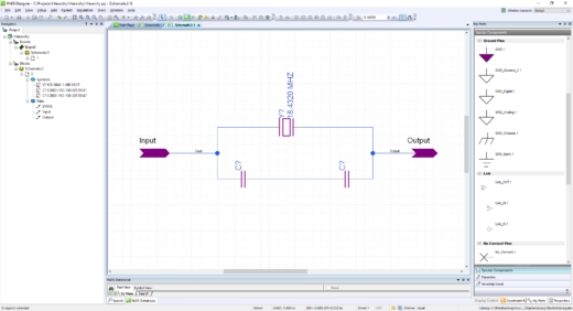
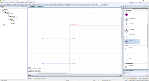
1. Create lower-level schematic with ports for input and output
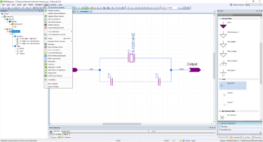
2. Create a composite symbol
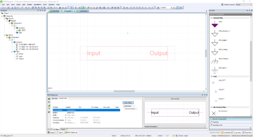
3. Place in top-level schematic
Top Down
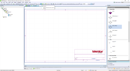
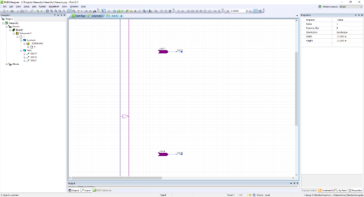
- Create a block in top-level schematic
2. Add connectivity to the block
3. Push into block to create lower-level schematic in block
Each method produces the same end product – it all comes down to preference. Typically, Bottom Up thinkers like to plan out and design every step of the way while Top Down thinkers like to conceptualize the entire project before diving into designing each block. Either way, you’re finishing up your projects with a more organization and efficiency.
Thanks for reading and see you next time for more on the ABCs of PCBs.
-Shivani Joshi
