ABCs of PCBs – D for DRC
Welcome to ABCs of PCBs – a blog series to help new engineers learn about the world of Printed Circuit Boards. I’ll be covering topics from general engineering concepts to PCB design specific rules. As this is a ‘basics’ blog, I’ll keep the content software independent, but any visuals will be from the Mentor PADS Professional PCB suite.
If you missed the last post in this series: ABCs of PCBs – C for Constraints click here!
I started this series off with A for Analysis; covering its importance and a few examples of techniques to use when designing PCBs. There, I introduced design rule check (DRC). Now, let’s take a deeper look at how these rules can aid in your design process.
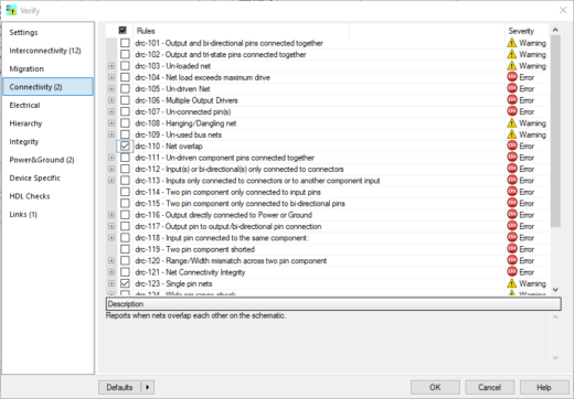
DRC, simply put, are rules you can use to check your design. You may see tools with built-in DRCs that can be parameterized by the user and the option to create your own rules based on design requirements. The goal of these rules is to identify electrical, physical, or logical violations that may affect the integrity of the design. It’s important to note that running a DRC will flag violations; not fix them. It’s up to you whether the violation is worth addressing. You’ll typically receive an output of DRC warnings or fatal errors from which you can take a few different courses of action:
- Fix the violation by adjusting your design until it passes the rules
- Ignore the violation and use caution as you proceed with the design process
- Adjust your rules
The rules can help flag potential issues in signal integrity, electromagnetic interference (EMI), clearance, naming formats, etc. You can run rule checks at any point in the design process. The following are some rules you may find beneficial to use on your designs:
Component polarity
This will check that polarized components have their positive pin connected to a voltage greater or equal to the voltage of their negative pin. A slight slip in component placement during schematic entry can result in a failed design. Running this type of check early can alert you to potential failures.
Net name check
Reports nets with the same name, but different letter case or name delimiters. For example, Data9 and Data[9] may mean the same thing to you, the logical thinking human, but software doesn’t see it that way. This type of inconsistent naming convention leads to confusion and usually a mistake in layout.
Dangling via
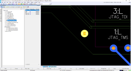
A dangling via is any via that is not properly connected on multiple layers to a trace or plane. Maybe you added a via during layout thinking you’d need it to avoid overlap, but later found an efficient way around it. Now you have this dangling via – unconnected on the layer you decided it wasn’t necessary and connected on the other end to a trace on the layer you had originally connected it to. This may not be the easiest error to spot on your own.
There are many DRCs that can assist with many different types of projects. It’s important to take the time to set these rules early in the design process and check them often to make sure you’re producing a quality design.
Thanks for reading and see you next time for more on the ABCs of PCBs.
-Shivani Joshi


