PCB Routing Solutions: Introduction
This is the first of a series of blog topics related to routing PCBs
My name is Charles Pfeil and my role at Mentor Graphics is one in which I always have a primary focus on routing technology and methods – although I do get involved in numerous other projects. I began in this industry working my summers in high school inspecting Ruby-Lithe designs for scratches and repairing them. Sounds rather antiquated? Indeed, this began in 1966 (some would say “way back” in 1966). I went to college to study architecture but soon realized that my passion for PCB design was so strong that I should pursue that instead.
After years of working as a job-shopper designing boards, I opened my own design service bureau, Sunshine Design. We started out with manual design and tape-ups. I still have some of those Mylar sheets with black tape-ups if anyone knows of a museum that might be interested them…I suddenly feel very old. In 1978, we made the change from manual design to CAD after getting two Racal-Redac Minis. During this transition, we lost all our customers who weren’t interested in CAD data. Fortunately, we were able to hook up with some customers who also used the Racal-Redac systems. At that point, CAD routing technology, both manual and automatic, became of great interest to me.
Since then I have worked at Racal-Redac, ASI, Cadence, Intergraph, VeriBest and Mentor Graphics. This industry has been very good to me and my career. I am grateful for all the wonderful people that I have met and worked with over these years.

My goal for this blog is to provide meaningful discussion of routing problems and their solutions. Over the years the routing task has become much more complicated, not only due to evolving component and fabrication technology, but also the need to fulfill high-speed requirements and manage the signal integrity concerns. I look forward to hearing your ideas and methods and hope that the discussions we have will help better equip us to solve the routing challenges that we face.
Here are some topics I look forward to discussing with you:
- Length of time needed to manually route a design
- Difficulty of phase match tuning
- The dense, tangled netlines between BGAs are hard to route
- The need to center traces between vias in BGA fanout array
- Fanout pattern complications and the difficulty of adding them
What challenges are you encountering? Are there any topics you would like me to add to my list?
Comments
Leave a Reply
You must be logged in to post a comment.


Actually, I am not sure how much to match the length of time per frequency.
To Brian Yu,
I asked Patrick Carrier of Mentor to provide some help with your comment, “Match length requirements vary between different kind of signals. DDR3, for example, requires tighter matching per byte lane, and the amount of matching should typically be in the 10s of picoseconds because the bus margins are typically on the order of hundreds of picoseconds. That equates to matching ~100mils. If we look at high-speed differential signals, on the other hand, they require very close matching to keep their edges aligned. If they have 50ps edges, that means there should be less than 5ps of skew between their positive and negative sides, which means length-matching tighter than 30 mils. Actually, it is probably best to keep differential pairs matched to within 5 mils to maximize the amount of margin.”
I would like to be able to specify certain pins as flexible or specify the pinout using constraints and for the placement algorithm to automatically swap nets around to optimise the routing.
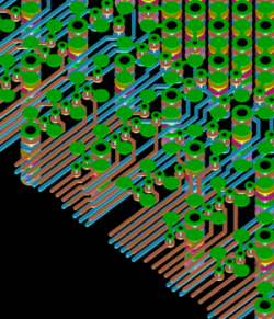
How did you get the 3D picture in the post above? Is that a “view” in Expedition?
To Jack:
The image was created using the Expedition PCB 3D Viewer.
Charles