Reflections from Siemens EDA User2User Forum in Noida
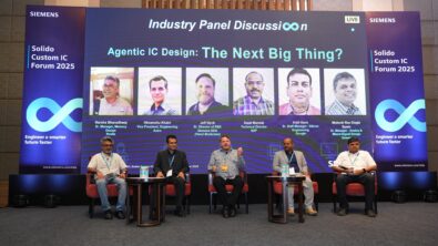
I recently had the privilege of representing the Solido Custom IC (CIC) team at the Siemens EDA User2User Forum 2025 in Noida, India on February 18.
This event brought together industry experts to explore innovative approaches to today’s most pressing chip design challenges and provided an ideal platform for knowledge sharing across the Siemens EDA ecosystem.
Solido CIC Team Presentations
The Solido CIC platform provides AI-powered design and verification solutions including S-Edit, L-Edit, Solido™ Design Environment, Solido™ Characterization Suite, Solido™ IP Validation Suite, and Solido™ Simulation Suite.
Our Solido CIC team delivered three presentations covering simulation, design environment, IP validation, and characterization solutions.
Each session also included testimonials from customers who shared their own experiences implementing the tools and the practical benefits they’ve seen in their workflows.
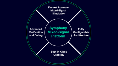
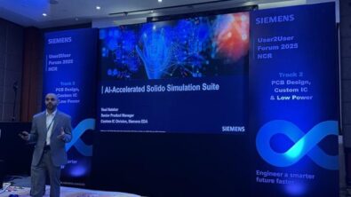
Supercharged high precision Custom IC Verification with AI-accelerated Solido Simulation Suite – Presented by Neel Natekar
My presentation demonstrated how our AI-accelerated Solido Simulation Suite is the industry’s most advanced simulation solution for SPICE, FastSPICE, and mixed-signal verification, supporting analog, RF, memory, library IP, and system-on-chip (SoC) applications.
Key takeaways: These simulation technologies deliver order-of magnitude speedup over other simulators, are certified by leading foundries, seamlessly integrate with signoff flows, and are optimized for cloud deployment.
Accelerating SPICE-accurate verification with production-proven AI from Solido Design Environment – Presented by Mohamed Atoua
This presentation focused on Solido Design Environment, and how it seamlessly integrates AI-powered variation analysis technologies to provide brute force-accurate 3 to high-sigma verification. Attendees also heard how it includes new Solido Additive Learning technology that leverages retained AI models to make faster and smarter decisions accelerating variation analysis for iterative workflows.
Key takeaways: The silicon-proven AI technologies in Solido Design Environment provide SPICE-accurate results, are orders-of-magnitude faster and are used in production by most of the top semiconductor companies today.
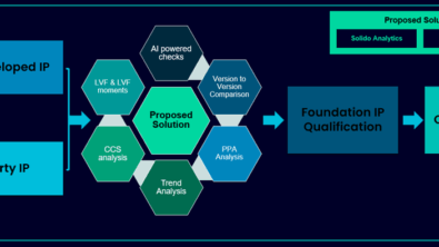
Accelerate SoC tape out schedules with production-ready IP & library views from AI-powered Solido Characterization Suite and Solido IP Validation – Presented by Sathishkumar Balasubramanian
This session covered Solido tools that focus on IP QA. Solido Characterization Suite is an AI-powered solution for library generation and validation and analysis. Solido IP Validation Suite is a comprehensive IP QA framework for in-view, cross-view, and version-to-version IP validation across all IP types and industry design views
Key takeaways: Solido Characterization Suite can perform accurate analysis of diversely sourced libraries across IP providers thereby helping designers optimize IP selection without having to run time and compute-intensive flows. Solido IP Validation suite ensures production sign-off quality IP QA for both IP providers and integrators.
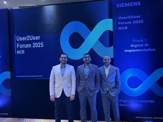
Mohamed Atoua, Sathishkumar Balasubramanian, and Neel Natekar at Siemens EDA User2User Forum in Noida
Insights from Noida User2User Forum
The event highlighted several important industry trends:
- As AI is becoming more pervasive in IC design and verification, it is crucial to ensure it is verifiable, usable, generalizable, robust, and, above all, accurate. This was eloquently summarized in the industry keynote by Mr. Amardeep Punhani, Senior Director R&D and Noida Site Head for NXP Semiconductors, who emphasized the essential need to develop safe, secure, and sustainable AI for systems, as well as systems for AI.
- IC designers and CAD engineers are encountering a growing number of challenges stemming from technology node scaling, the increasing complexity of IC designs, and the diverse requirements of various target markets.
- The rising complexity of IC designs is driving the industry to increasingly adopt the “shift-left” strategy where key verification and validation processes are executed earlier in the design flow, as highlighted by Mr. Ruchir Dixit, Vice President and India Country Manager for Siemens EDA, during his keynote session.
Beyond the technical sessions, the event provided valuable networking opportunities with customers and industry peers. The discussions with other attendees provided real-world insights into emerging market needs and highlighted several ways we might collaborate going forward.
Presentations from our partners, including ST Microelectronics and NXP, highlighted how our product enhancements enable them to optimize Power, Performance, and Area (PPA), significantly reduce design and verification cycles, and prevent costly design re-spins, resulting in substantial time and cost savings.
I thoroughly enjoyed representing Solido CIC at the Noida User2User Forum. The conversations, questions, and feedback we received were invaluable. Our team is excited to continue these discussions and demonstrate our solutions at upcoming Siemens EDA events.
Next stop on our calendar:
- User2User Europe – Munich, Germany | May 13, 2025
- User2User North America – Santa Clara, CA | May 20, 2025
See you there!