Another breakthrough in Semiconductor Industry engineered by Intel Foundry

Ever since I got my first computer, I eagerly anticipated the announcement of each new Pentium processor from Intel. These processors, renowned for their impressive computational power, significantly reduced boot times and efficiently ran the operating system. Most importantly, they dramatically improved the visual experience of playing video games on a PC, especially 3D racing games. The in-game scenes, which emulated the real world, captivated countless children and even adults. It was magical how these processors could create an alternate reality within such a small chip.
Yes, Intel is such a legendary company, Intel has been instrumental in advancing chip manufacturing and design technology over the past 60 years. The company’s relentless focus on semiconductor progress began with SRAM and DRAM, and quickly expanded to the central processing unit (CPU) business in the 1980s, coinciding with the rise of personal computers. Intel’s founders, including Andrew Grove and Gordon Moore, are highly respected in the semiconductor industry. Gordon Moore, in particular, is known for his industry prediction known as “Moore’s Law,” which states that ‘the number of transistors in an integrated circuit (IC) doubles approximately every two years.’ This law has guided the development of the semiconductor industry to this day. Intel began adhering to this rule as early as the 1970s. Their manufacturing process started with a 10um transistor size in the 1970s, which was reduced tenfold to 1um in the 1980s, and further reduced to 22nm in the 2010s. The reduction in transistor size increases the density of transistors per unit area, allowing for more circuit functionality on a single chip. This leads to faster switching times and higher frequencies, enhancing the chip’s computational capacity while operating at lower supply voltages.
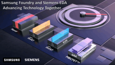
For a long time, Intel’s process technology was considered the world’s most advanced semiconductor manufacturing. However, this technology was not disclosed to the broader industry and was solely dedicated to the manufacturing of Intel’s processors. In 2021, Intel redefined its foundry initiative by creating Intel Foundry Services (IFS) to revitalize the semiconductor industry’s increasing demands for high performance process technologies. IFS unveiled their advanced process technologies to customers worldwide. Intel’s most advanced Intel 18A incorporates an advanced RibbonFET Gate-All-Around (GAA) transistor architecture and proprietary PowerVia backside power delivery technologies. These innovations, part of the late-FinFET generation, assist customers in optimizing the density and performance of their products. They target applications in High Performance Computing (HPC) and mobile devices in this AI era. In addition to these advancements, Intel’s process technology portfolio includes planar and FinFET technologies, such as the Intel 3 and Intel 16 process nodes. These technologies further demonstrate Intel’s commitment to innovation and excellence in semiconductor manufacturing.
Siemens Digital Industries Software, Intel Foundry’s trusted partner, has announced the certification of its Analog FastSPICE (AFS) platform and Calibre® nmPlatform with Intel’s 18A and Intel 16 process technologies. This certification provides a precise verification platform for IC designers working in the fields of analog, RF, custom digital, and mixed-signal circuits. In addition, Intel’s 18A and 16 process technologies are now equipped with the Open Model Interface (OMI), enabling precise modeling and reliability analysis. By joining the Intel Foundry ecosystem, Siemens can offer a comprehensive verification platform that enhances product cycle efficiency and boosts design flexibility across various product applications. Read the public announcement here: Siemens qualifies industry-leading IC design solutions for Intel Foundry processes
To learn more about the Analog FastSPICE (AFS) platform of Siemens Custom IC Verification technologies, visit https://eda.sw.siemens.com/en-US/ic/verification-and-validation/custom-ic-verification/