Silicon Valley IC Packaging Seminar Validates Growing Proliferation of FOWLP
If you’re interested in High Density Advanced Packaging (HDAP), our recent, focused seminar at Mentor Graphics’ Fremont campus was the place to be. Great attendance and lots of audience engagement around the challenges and advantages of using HDAP. And, with future opportunities for HDAP in almost every market segment, it was no surprise to see some of the biggest companies in electronics in attendance, from chip makers to electronic systems producers.
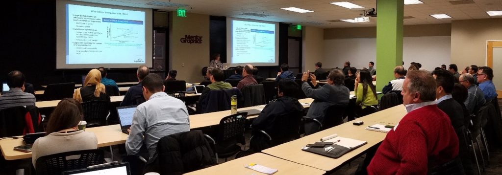
Jan Vardeman, President and Founder of TechSearch International, shown below, provided a broad insight into Fan Out Wafer Level Packaging (FOWLP) and other HDAP methodologies such as 2.5D. Mentor talked about its FOWLP/HDAP solution and provided live demonstrations of key technology areas, many of which are unique to Mentor’s Xpedition and Calibre product families.
Key takeaways were that FOWLP is real, growing, and expanding into many new market segments. Cross substrate integration, prototyping, and optimization are key to HDAP and FOWLP adoption and tapeout success. Read our white paper to learn more. To be invited to our next HDAP seminar, leave a note below.


