Behind the Design: Qualcomm Technologies Inc.
This is the fourth post in a series showcasing the winners of the 2014 Technology Leadership Awards. View the previous ones here.
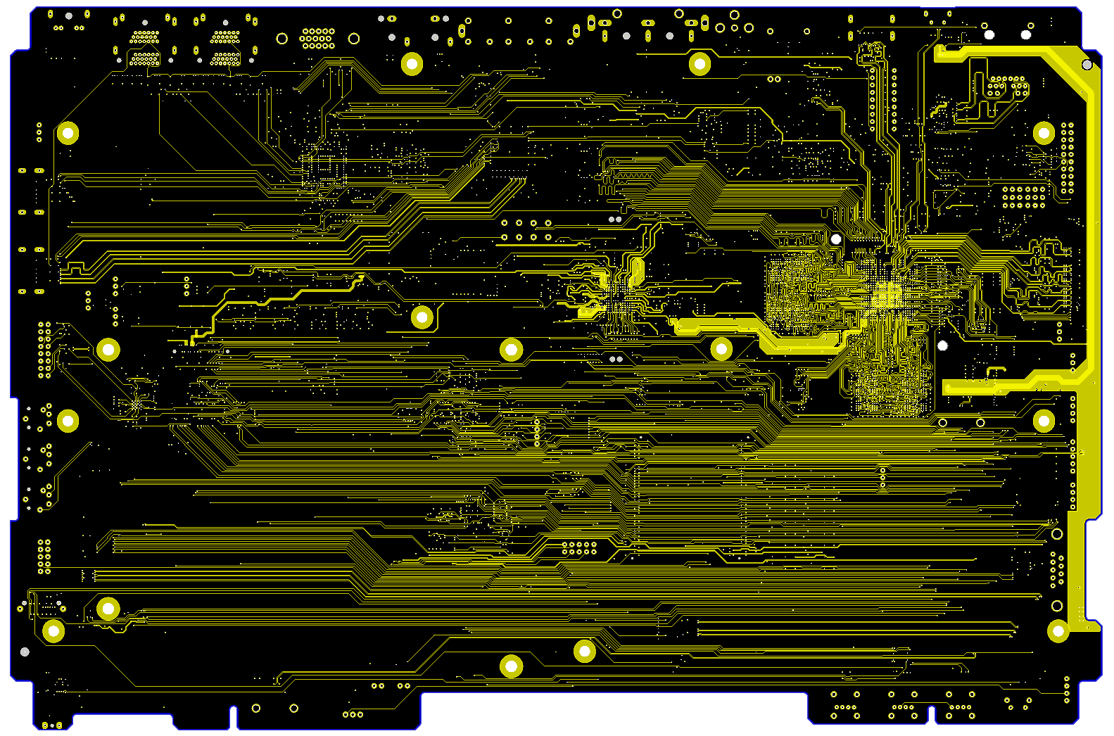
First place winner in the Consumer Electronics & Handheld category: Qualcomm, United States
![]()
Design: a Quad-core APQ (application processor Qualcomm) targeting the tablet/netbook market segments
Design team: Larry Paul, Sanat Kapoor, Stephen Baker, Danlin Xiang, Michael Tex
Design challenges:
- Quad-core Krait, A320 3DGfx, Dual Channel PCDDR3/3L + LPDDR2 PoP option, integrated GPS SS w/Gen8A-Lite Nav core, 1080p HDMI Video, Media Processor, SATA Gen1, and PCIe 2.0
- To maintain cost constraints, a through-hole 8-Layer stackup with no HDI layers needed to be used
- Trace width dimensions of under 3th
- Multidiscipline collaboration was utilized:
- PCB Layout, Package & APQ were designed together with a co-design process and collaborated across the PCB, package and IC design teams
- The power and signal integrity group helped with simulations and design feedback; multiple rounds of power simulations and memory simulations were needed to optimize the package and PCB routing
- Design for reuse – the second memory circuit was designed to be copied and replicated; memory circuit can be single or dual ranked to support four memory banks
- Eight DDR comps mounted four on each side; sharing thru via fanouts
- 97 percent of the design was high-speed nets, with close to 9,000 connections
Design tools and team comments:
- Xpedition® Enterprise and Package Integrator
- Package Integrator is used at Qualcomm to help optimize pin definition on the APQ.
- “Mentor’s Package Integrator tool allowed us to manage multiple rounds of signal assignment evaluation across teams without loss of data. The design was initially worked out in a co-design study through PCB Layout. Near completion the circuit placement and routing was copied to a customer reference design to re-use and quickly route 80% of the traces. This allowed us to build a product quickly and fabricate a working design with no design spins.”
Judge’s comments:
- The intense activity around the RAM is very impressive.
- Good team effort across multiple disciplines. This is a tight design considering that is utilizes standard technology instead of HDI.
About the Technology Leadership Awards
Started in 1988, this program is the longest running competition of its kind in the electronic design automation (EDA) industry. It recognizes engineers and designers who use innovative methods and design tools to address today’s complex PCB systems design challenges and produce industry-leading products. See the full list of 2014 winners here.


Comments
Leave a Reply
You must be logged in to post a comment.
Respected Sir,
I am the student of Sinhgad Institute (Kondhwa BK) Pune
Appearing M.E.(2nd yr) I am interested to doing projected in skin disease but I not get the whole information about the Hand-held probe used to measure impedance which u show in u r 2003 IEEE paper.
please help me to know the detail information of that probe, like where manufacturing and how it will buy in the market & approximate cost of that equipment.
Pravin
As your comment really has nothing to do with this Blog, I am unsure what you are requesting, and if you are requesting it from the correct location.
Otherwise, the best location to find info on Impedance Probes for manufacturing would be with your local PCB Fabrication Facility. Their engineering departments should be able to provide you with the information you are requesting.
Thanks,
Vern