Part 2: The 2010 Wilson Research Group Functional Verification Study
Design Trends (Continued)
In Part 1 of this series of blogs, I focused on design trends (click here) as identified by the 2010 Wilson Research Group Functional Verification Study (click here). In this blog, I continue presenting the study findings related to design trends, with a focus on embedded processor, power management, and clock domain trends.
Embedded Processors
In Figure 1, we see the percentage of today’s designs by the number of embedded processor cores. It’s interesting to note that 78 percent of all non-FPGA designs (as shown in green) contain one or more embedded processors and could be classified as an SoC, which by nature is complex to verify. Yet, even 55 percent of all FPGA designs contain one or more embedded processors.
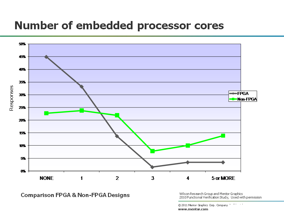
Figure 1. Number of embedded processor cores
Figure 2 shows the trends in terms of number of embedded processor cores for non-FPGA designs. The comparison includes the 2004 Collett study (in orange), the 2007 Far West Research study (in blue), and the 2010 Wilson Research Group study (in green).
We are unable to show the FPGA trend data since none of the prior industry studies contained FPGA participates. However, future studies should be able to show FPGA trends since the 2010 Wilson Research Group study did contain FPGA participants.
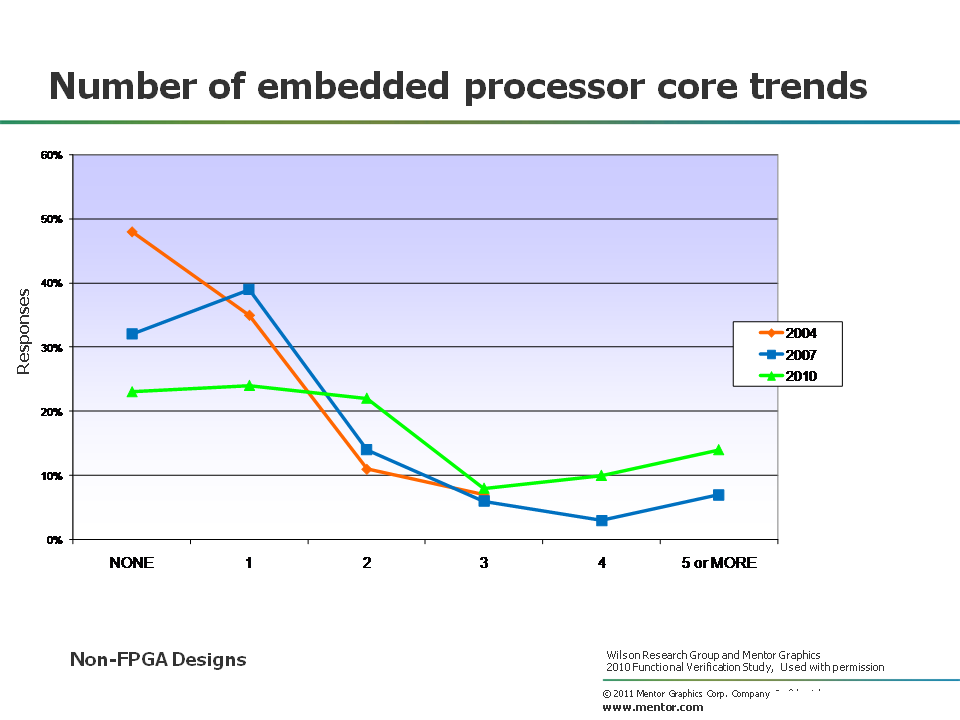
Figure 2. Number of embedded processor core trends
The median number of embedded processor cores in 2004 was about 1.06. This number increased in 2007 to 1.46. Today, the median number of embedded processor cores was found to be 2.14.
Another interesting analysis on the study data is to partition it into design sizes (for example, less than 1M gates, 1M to 20M gates, greater than 20M gates), and then calculate the median number of embedded processors per partitioned set. The results are shown in Figure 3, and as you would expect, the larger the design, the more embedded processor cores.
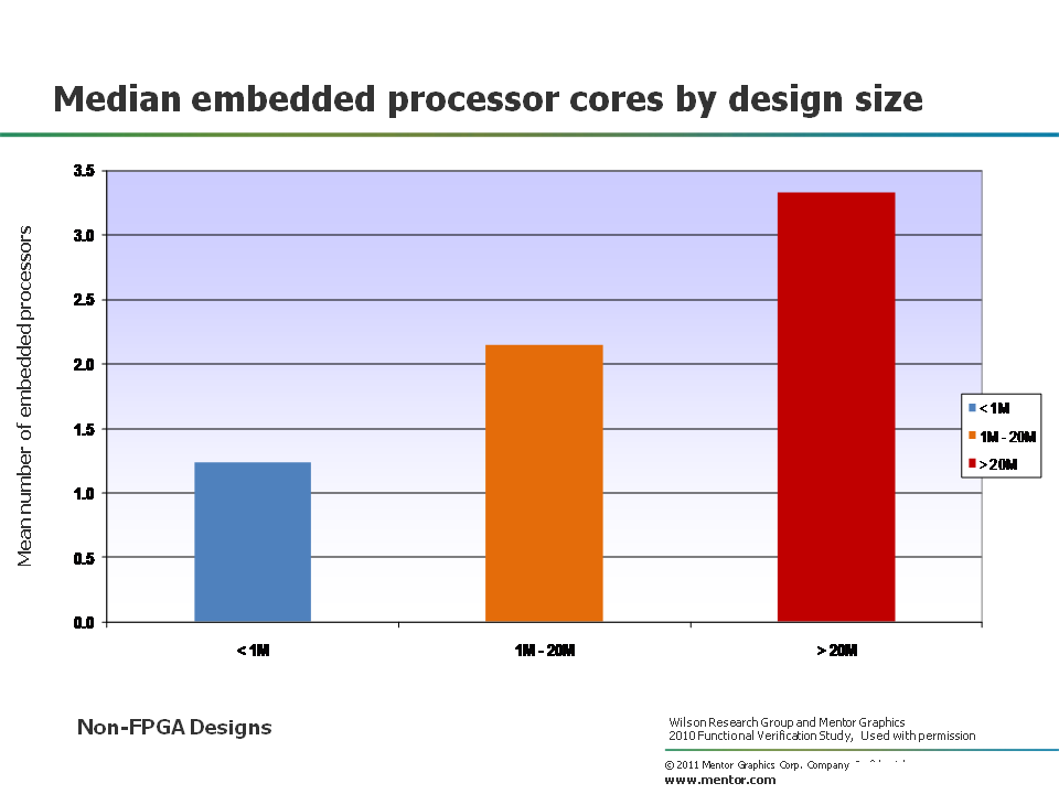
Figure 3. Median embedded processor cores by design size
Platform-based SoC design approaches, containing multiple embedded processor cores with lots of third-party and internally developed IP, have driven the demand for common bus architectures. In Figure 4 we see the percentage of today’s designs by the type of on-chip bus architecture for both FPGA (in grey) and non-FPGA (in green) designs.
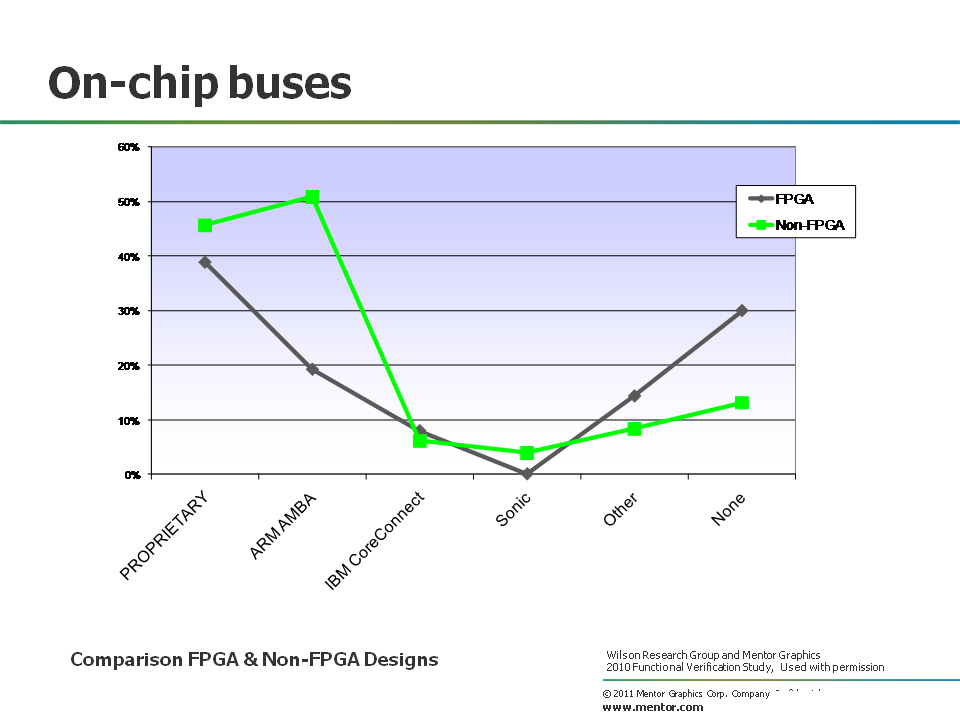
Figure 4. On-chip bus architecture adoption
Figure 5 shows the trends in terms of on-chip bus architecture adoption. The comparison includes the 2007 Far West Research study (in blue), and the 2010 Wilson Research Group study (in green). The study did not partition out the various ARM AMBA bus architectures between the 2007 and 2010 studies. However, it is interesting to note that there was about a two hundred and forty one percent increase in designs using the ARM AMBA bus architecture.
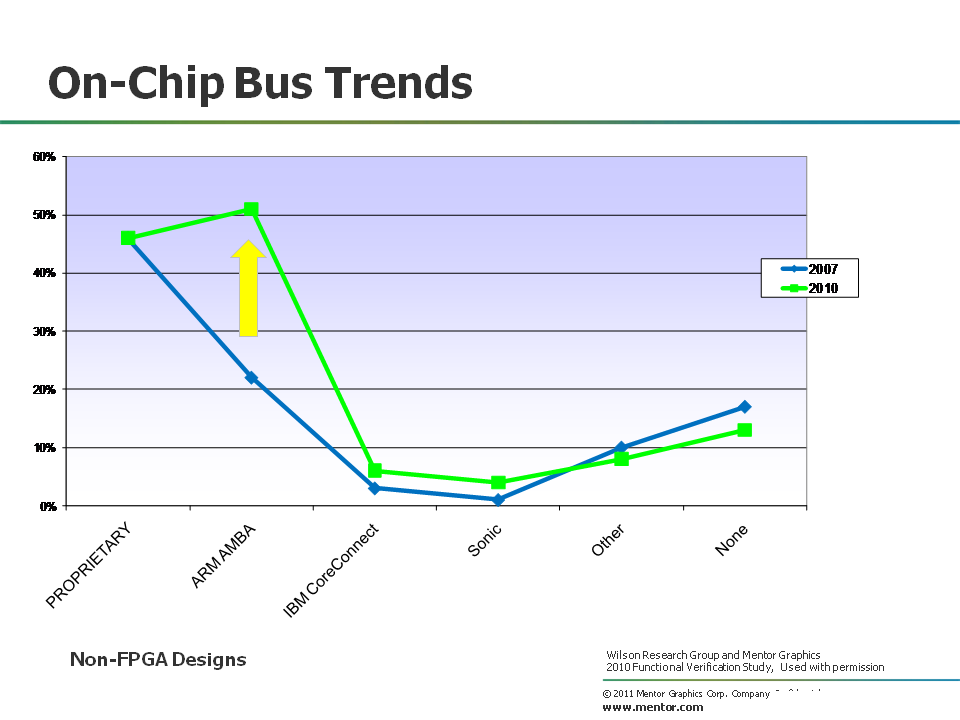
Figure 5. On-chip bus architecture adoption trends
One interesting way to analyze the study data is to partition the responses by geographical region. The results are shown in Figure 6. The regional comparison are North America (in blue), Europe/Israel (in green), Asia minus India (in orange), and India (in red).
Notice how Asia appears to lead the world in the development of designs containing ARM processors when compared to the rest of the world.
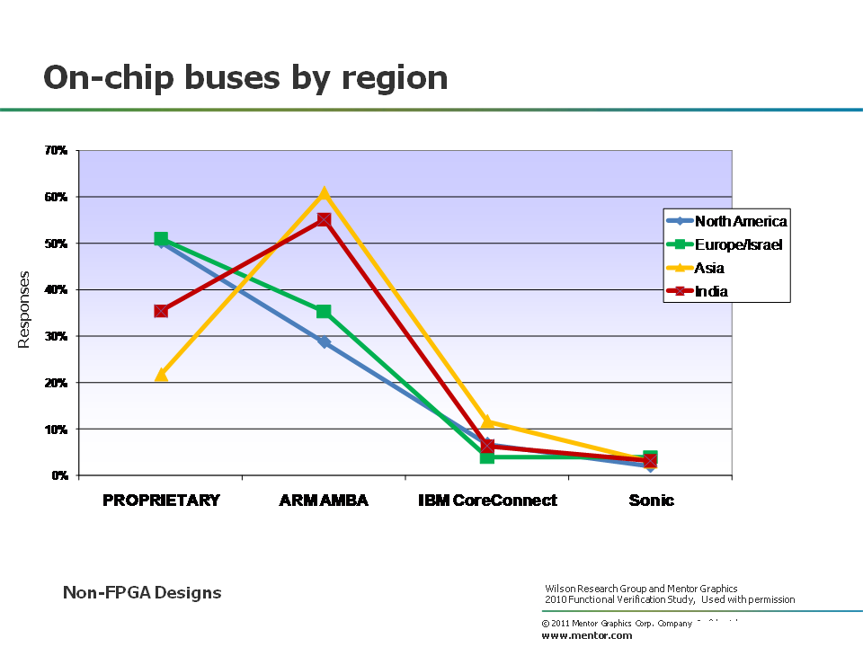
Figure 6. On-chip bus architecture adoption by region
Another interesting analysis is to partition the data by design sizes. The results are shown in Figure 7 with the following design size partitions: less than 1M gates (in blue), 1M to 20M gates (in orange), and greater than 20M gates (in red).
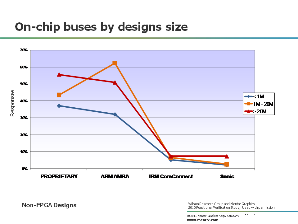
Figure 7. On-chip bus architecture adoption by design size
In Figure 8 we see the percentage of today’s designs by the number of embedded DSP cores for both FPGA designs (in grey) and non-FPGA designs (in green).
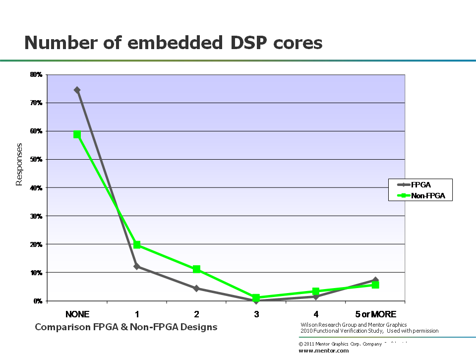
Figure 8. Number of embedded DSP cores
Figure 9 shows the trends in terms of the number of embedded DSP cores for non-FPGA designs. The comparison includes the 2007 Far West Research study (in blue), and the 2010 Wilson Research Group study (in green).
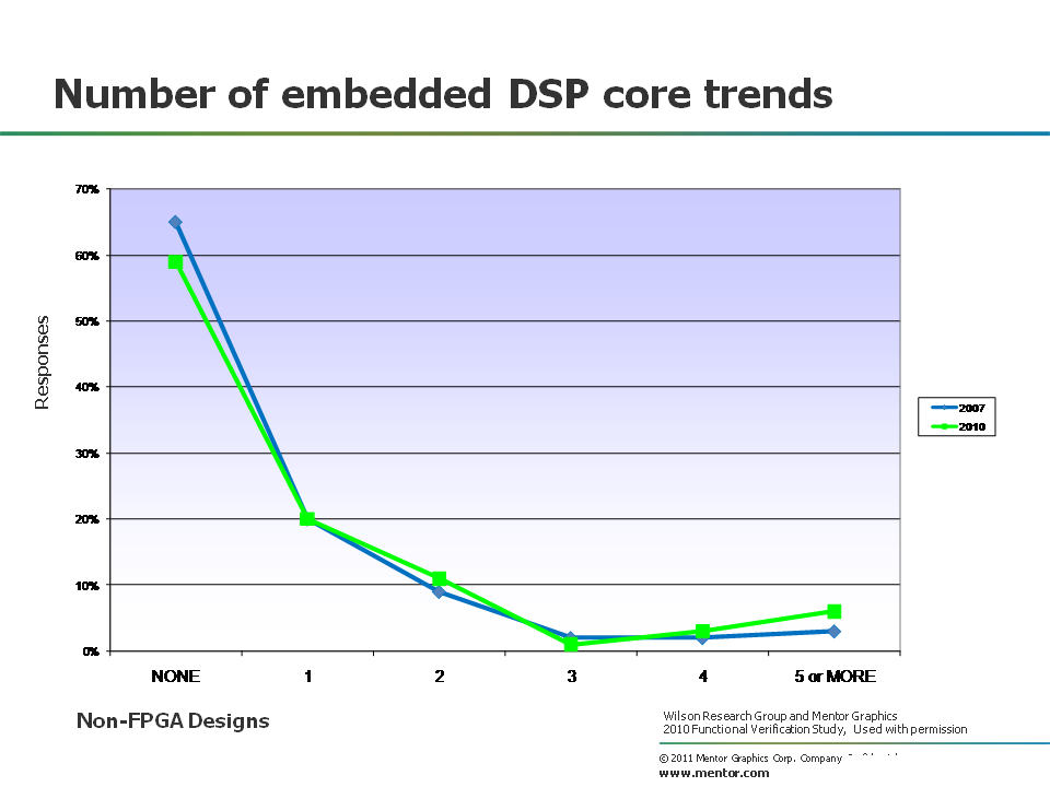
Figure 9. Number of embedded DSP core trends
Independent Asynchronous Clock Domains
Figure 10 shows the percentage of design developed today by the number of independent asynchronous clock domains. The asynchronous clock domain data for FPGA designs are shown in grey, while the data for the non-FPGA designs is shown in green.
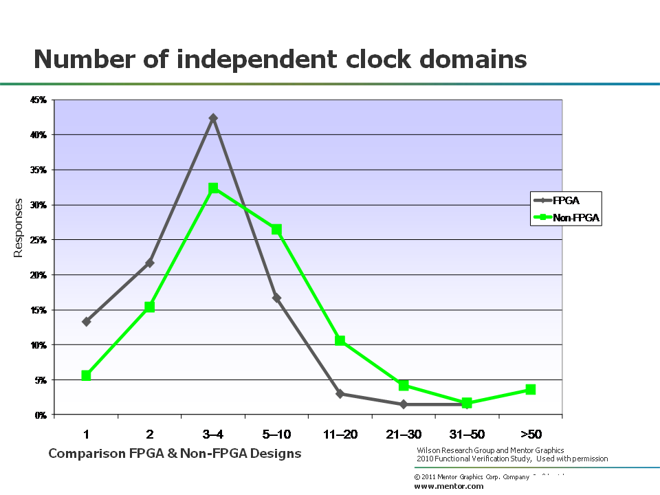
Figure 10. Number of independent asynchronous clock domains
Figure 11 shows the trends in number of independent asynchronous clock domains for non-FPGA designs. The comparison includes the 2002 Collett study (in orange), the 2004 Collett study (in pink), the 2007 Far West Research study (in blue), and the 2010 Wilson Research Group study (in green).
It’s interesting to note that, although the number of clock domains is increasing over time, the sweet spot in terms of number of independent asynchronous clock domains seems to remain between two and 11 clock domains, and hasn’t changed significantly in the past nine years.
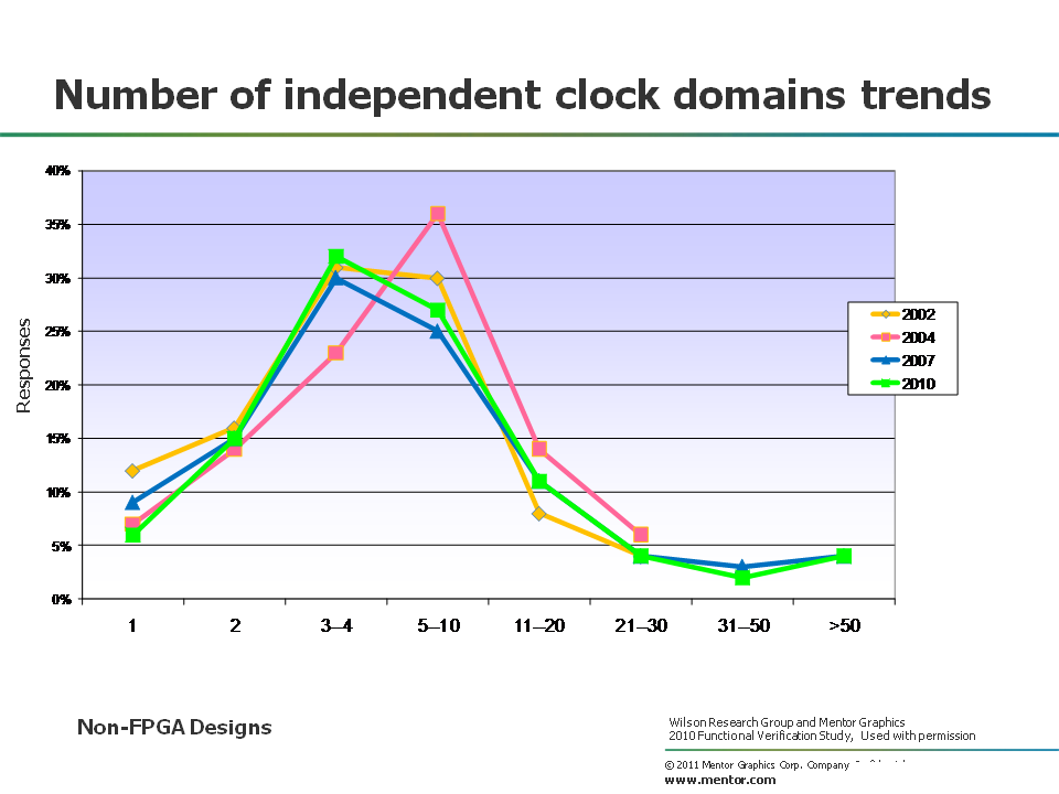
Figure 11. Number of independent asynchronous clock domain trends
Figure 12 partitions the study data by geographical region, and shows the median calculation for the number of independent asynchronous clock domains. The regional comparison are North America (in blue), Europe/Israel (in green), Asia mimus India (in orange), and India (in red).
Notice how Asia appears to lead the world in the median number of independent asynchronous clock domains.
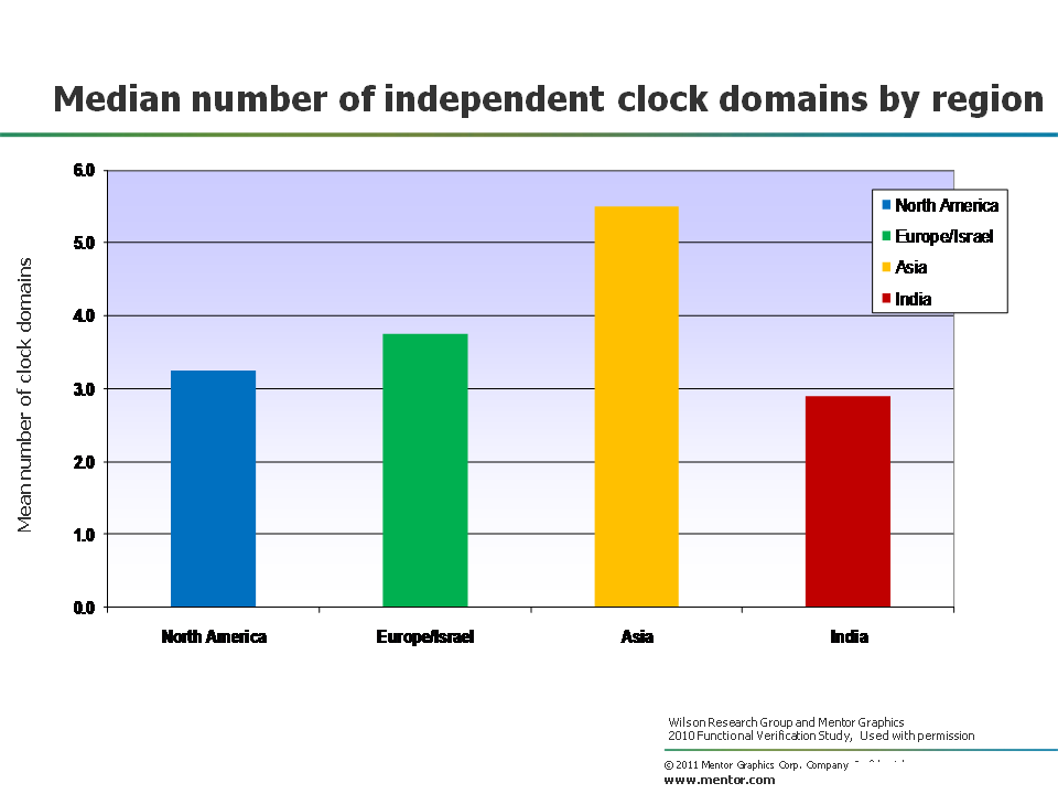
Figure 12. Median number of independent clock domains by regions
Figure 13 provides a different analysis of the data by partitioning the data into design sizes, and then calculating the median number of independent asynchronous clock domains. The design size partitions are represented as: less than 1M gates (in blue), 1M to 20M gates (in orange), and greater than 20M gates (in red).
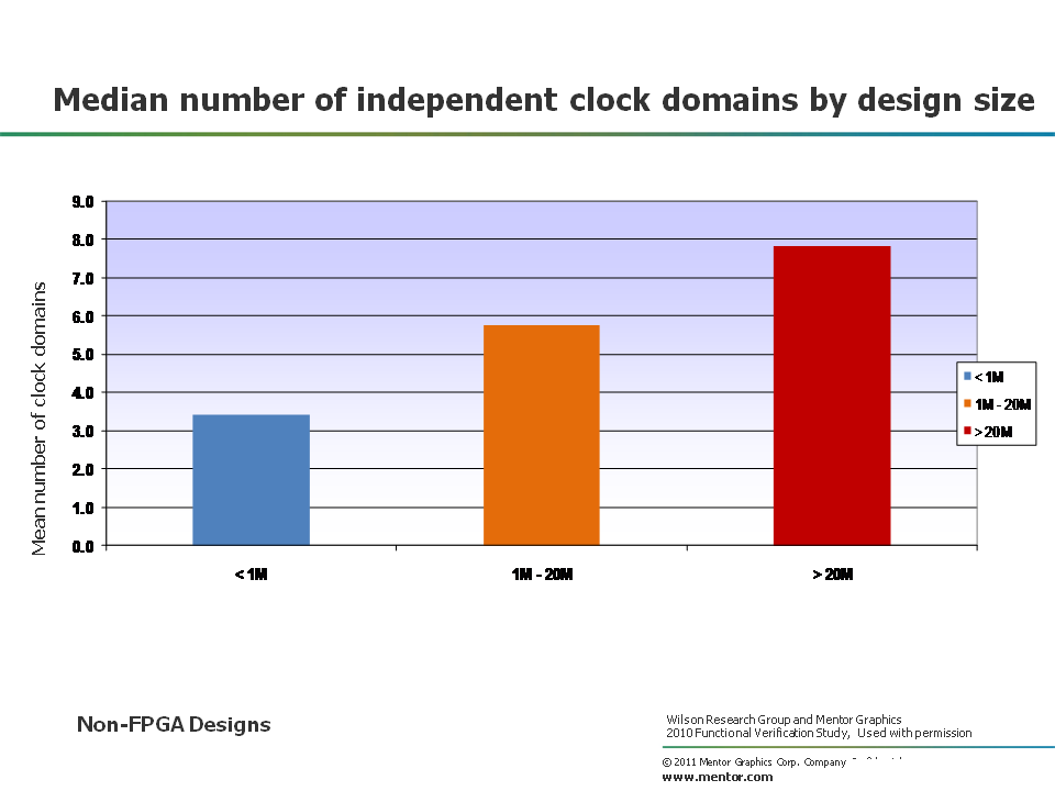
Figure 13. Median number of independent clock domains by design size
Power Management
Figure 14 shows the percentage of designs that actively manage power by process geometry size. You will note that at 45nm, the study indicates that there is an increasing need to actively manage power.
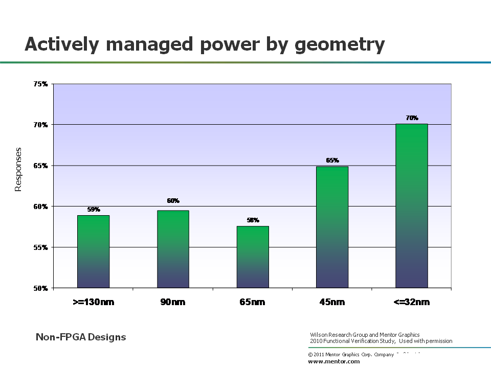
Figure 14. Designs that actively manage power by process geometry
The size of the design, regardless of its process geometry, influences the decision to actively manage power, as shown Figure 15. The design size partitions are represented as follows: less than 1M gates (in blue), 1M to 20M gates (in orange), and greater than 20M gates (in red).
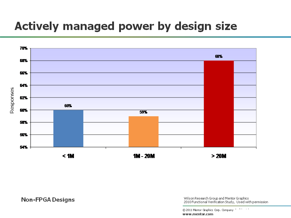
Figure 15. Design that actively manage power by size
Although there are many techniques that are used to manage power, Figure 16 shows the percentage of use for the top eight techniques that were identified through the study. It’s important to note that many designs will implement multiple power management solutions on a single chip.
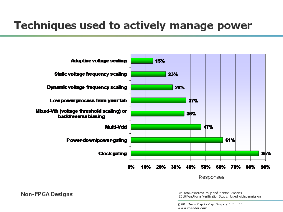
Figure 16. Top eight techniques used to actively manage power
In my next blog (click here), I’ll present data on design and verification reuse trends.


Comments
Leave a Reply
You must be logged in to post a comment.
Hi, Harry – just waiting for those design& verification language trends!
Hi Cliff – Be patient. The data is coming. I still have a lot more blogging to do!
Hi Harry, thanks for sharing the study results! I suppose the complete study (e.g. as PDF) will not be public & free of charge in the near future? Best regards
Hi Christoph – This has not been decided yet. Best Regards
Cliff, did you look at some of this data which appeared in Wally’s DVCon keynote? Slide 53 has some of the info on Design & Verification languages. You can find it at http://www.mentor.com/company/industry_keynotes/upload/DVCon-2011.pdf#page=53. (Wally’s keynote presentation does not include information on the languages the FPGA designers use.)