Meet aggressive time-to-market for AI chips by slashing DFT time
Semiconductor companies are racing to develop AI-specific chips to meet the rapidly growing compute requirements for artificial intelligence (AI) systems. AI chips from companies like Graphcore and Mythic are ASICs based on the novel, massively parallel architectures that maximize data processing capabilities for AI workloads. Others, like Intel, Nvidia, and AMD, are optimizing existing architectures like GPU, CPU, and FPGA to keep up with the performance requirements of AI systems. All the AI chip designs are very large (billions of gates), have a large number of replicated processing cores, and use distributed memories…
Success for these companies depends on getting their AI chips to market quickly. Every part of the design flow—including everything needed for IC test and silicon bring-up—needs to work towards the goals of getting high-quality, working silicon into customer’s hands as soon as possible.
With time-to-market as a top requirement, three features of a DFT solution emerge:
- Exploit AI chip regularity
- Perform DFT insertion and verification in RTL
- Eliminate DFT-to-test iterations during silicon bring-up
These DFT techniques are already in use at many leading semiconductor companies and have proven to achieve up to 10x faster ATPG with 2x pattern reduction and radically accelerate bring-up, debug, and characterization of AI chips.
Exploit AI chip regularity
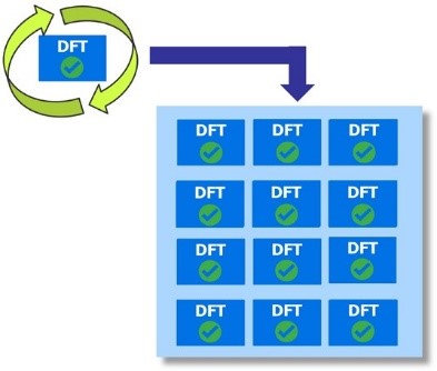 Exploiting the AI chip regularity involves completing all the DFT work—including test insertion, test pattern generation, and verification—just once at the core level. The complete, signed-off core is then replicated automatically to complete the chip-level DFT implementation. This approach takes DFT out of the critical path to tapeout, avoiding any impact on the project schedule.
Hierarchical DFT allows for core level sign-off, replication, and also core-level diagnosis. The core-level diagnosis significantly accelerates the process of diagnosis and failure analysis over chip level diagnosis. A Hierarchical DFT and pattern generation methodology aligns perfectly with the AI chip architectures, which contain repeated identical processing cores.
Other useful DFT techniques that allow users to optimize implementation to meet the AI chip test requirements include:
- Channel broadcasting, in which the same test data can be broadcast to all the identical cores
- Using a shared Memory BIST controller, where a single Tessent MemoryBIST controller is shared between multiple memories in multiple cores
- Using an embedded test compression (EDT) low power controller that allows more cores to be tested together without increasing the test power.
Perform DFT insertion and verification in RTL
DFT logic is traditionally inserted and verified in a gate-level design during or after synthesis. However, DFT insertion and verification in RTL is much faster because RTL simulation and debug is faster than gates-level and doesn’t require going through the synthesis step. RTL DFT insertion also allows for early I/O and floor planning of the chip. This process significantly shortens the design development cycle. Designers can achieve higher test quality in less time by performing all the DFT checking and fixing most testability issues at RTL before running ATPG.
Eliminate DFT-to-test iterations
Reducing the time spent on silicon bring-up is critical in getting ICs into the hands of customers. The traditional process of silicon bring-up typically involves the multiple iterations between the DFT domain and the test/ATE domain for pattern debug, characterization, test optimization, and test scheduling.
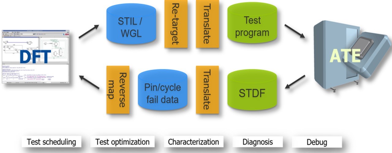
With a direct connection between the DFT and the ATE domains, the DFT engineers can perform the silicon-bring up themselves and the test engineers can run diagnosis without the help of DFT engineers. Connecting the DFT and ATE domains reduces silicon bring-up time from weeks to days.
In a new whitepaper, we expand on the characteristics and challenges of AI chips and go into details of the techniques to help meet aggressive time-to-market requirements of AI chips. The paper includes a section on practical application of hierarchical DFT and references to published results. Read the whitepaper to learn more.