Printed circuit board designs optimized for manufacturing
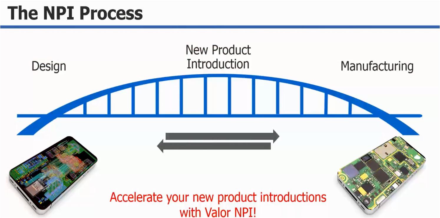
Watch the Digital Enterprise Factory Showcase Tour video blog series to experience the power of digitalization in manufacturing. Today, at the fourth stop on our tour, the experts will show you how the Valor New Product Introduction (NPI) application helps you accelerate your new product introductions.
Highlights of the video featuring Valor NPI:
-
- Optimize printed circuit board for yield, cost and reliability during the initial PCB design process
-
- Xpedition integration enables DFM concurrent with the design process
-
- Eliminate design spins caused by manufacturing issues
-
- Design and optimize panels for lowest material cost
Watch the video “PCB Designs Optimized for Manufacturing” to learn how to accelerate your new product introductions with Valor NPI.
Digital Enterprise Factory Showcase Tour – blog #3 in series
Integrated design & simulation for optimizing design solutions – blog #2 in the series
Introduction to the Digital Enterprise Factory Showcase – blog #1 in the series
This blog is co-authored by Zvi Feuer and Lisa Hartman, Siemens PLM Software.
Transcript of PCB Designs Optimized for Manufacturing:
The new product introduction process spans both the design and manufacturing of printed circuit boards. It requires clear and complete communication between the two. Mentor’s Valor NPI application software helps you accelerate your new product introductions. To improve any process, you always look to shift actions and decisions to the left as much as possible. With PCB design for manufacturing, best practices are to perform DFM, concurrent with the layout process.
From within Mentor Xpedition, we can export the design and launch Valor NPI. Here we can see the intelligent information such as layer copper weights, is automatically passed from Xpedition to Valor NPI. The analysis definition manager is used to easily set up the DFM constraints. We also make use of the intelligent information that comes over to tune the analysis based on critical attributes of the design.
In this first example you can simply set up the constraints to utilize copper weight and the layer position. Valor NPI has an ability to easily import various BOM files utilizing the BOM import wizard. Once the BOM is imported, we can run a match with the Valor parts library to automatically assign the part which includes data such as pin contact information. When applied to the EDA footprint, we run a full pin to pad analysis to check for proper solder joint.
We’re ready to run the fin analysis with the user has access to one thousand different check.
You can see the results have be categorized into eight different results types, indicated by the tabs on the right. We will drop into the edge type result first, we will select this example of a short sliver. Once we select the first issue, you can see it zooms into the issue, and Xpedition automatically synchronizes with Valor NPI, to make it easy for the designer to make the update in Xpedition. I will quickly make this fix, and be ready to move to the next issue.
Now for our second example, we will jump to the solder tab to look at the pin to pad issue. In this example you can see the actual pin of the device that came from the Valor parts library has a distance violation. There is inadequate space with this part, to achieve a proper solder joint. You can see the red boxes that pin of the part, while the green is copper. Hence the pin is not suited fully on the pad. With Valor NPI you can optimize your PCB designs for manufacturing during the initial design stage. For example you may have a spacing issue between circuits. But it is only critical if there are multiple instances or the link to violation is excessive. Once you’ve completed your analysis and optimized your design for manufacturing, you are ready to panelize the design. Simply select the desired panelization approach from the wizard into the desired parameter settings and let the system create for you, a simple fabrication panel, optimized for the lowest material cost.
Now that we have the panel, let’s automatically add the necessary features such as tooling holes, Fiducials, routs, breaktabs, with a single click using the rapid panel modeler. You can see as I turn on the top layer, we now have now have complete optimized panel. We are ready to generate our ODB++ output, which supports fabrication and assembly, while protecting your intellectual property. The single ODB++ container provides all the information necessary, to manufacture your optimized PCB.