A Little Goes A Long Way (But A Lot Doesn’t Go Much Further)
It has been almost 3 years since I started this blog and I hope you’ve found it as interesting as I have cathartic. Although I’m not as yet bereft of topic ideas, I thought this would be a good time to solicit a guest blog from industry. It was either that or a Simponsesque montage of previous posts. I covered the highly successful provision of FloTHERM models of power packages from NXP previously. Now I’d like to hand over to Chris Hill, NXP Applications Engineer, who will discuss diminishing returns in thermal design…
 Chris started work as an Applications Engineer at Philips Semiconductors in 1996, specialising in power MOSFETs. He remained at Philips whilst it became NXP Semiconductors and spends considerable amounts of his working life immersed in questions of a thermal nature. When not sat at his desk watching Profiles windows, he likes nothing better than plodding through muddy fields in the North of England.
As an Application Engineer for a major power semiconductor manufacturer, I spend a great deal of my working life worrying about how to remove heat energy from our MOSFET devices, and hence maintain safe device working temperatures. The majority of our products are surface-mounted, and so use the PCB as their heatsink. Common questions which therefore arise are “How much copper area should I use?”, “What is the influence of PCB layer count?” and “Should I use thermal vias?”. As you can probably imagine, it is impossible to give definitive answers to these questions, as there are so many other factors which contribute to the “thermal performance” of a device or devices mounted on a PCB. However, we do believe that it is possible to give our customers useful information about the relative performance of different PCB configurations, so that they can start to make informed choices about general PCB layout before going into a more detailed design phase.
So far we have produced two lengthy documents on this subject (generated from extensive use of FloTHERM), titled “AN10874 LFPAK MOSFET thermal design guide” and “AN11113 LFPAK MOSFET thermal design guide – Part 2” (will there be a Part 3? who knows…)
Whilst generating the data for Design Guide (part 1) an interesting trend started to emerge, and it is to that subject that I would like to turn. The graph below is reproduced from AN10874, p18, Fig 13.
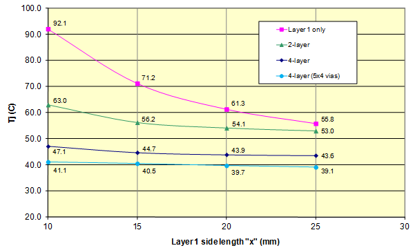 This graph illustrates the dependence of the temperature of a single device (TJ) on various aspects of PCB configuration. At this point, it helps to see the actual PCB setup:
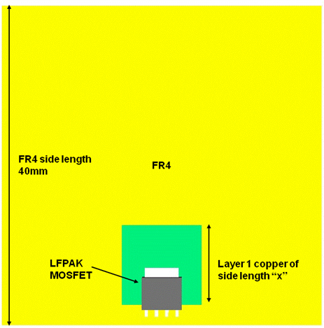
What we have here is a single MOSFET (in an LFPAK package) mounted on an FR4 PCB with fixed side lengths of 40 x 40mm. Device dissipation is 0.5W and ambient temperature is 20°C. We’re going to have a look at what happens to TJ when we vary the copper dimension “x” for various different PCB stackups i.e.
- Just the layer 1 copper on its own (pink line on the graph).
- With a fixed bottom copper layer of 40 x 40mm added (green).
- As 2., with internal layers (nominal 50% coverage) added (dark blue).
- As 3., with “thermal vias” added under the device (light blue).
So turning to the pink line (layer 1 only) line first, we can see that when x = 10mm (i.e. a top copper square of side length 10mm) the resulting device temperature (TJ) is 92.1°C or a temperature rise of 72.1°C above ambient (AKA an Rthj-a of 144.2K/W for those who prefer such things). If we now increase “x” to 15mm, we see a dramatic decrease in TJ to 71.2°C. That extra copper area has really helped, reducing TJ by around 22% compared to the original figure! So how about if we increase “x” by another 5mm? Do we see another similar improvement? Well, not really – TJ has dropped from 71.2 to 61.3°C which represents a decrease of 14%. This is still a useful result, but not as dramatic as before. Similarly, increasing “x” by another 5mm (to 25mm) yields a TJ of 55.8°C or a decrease of 9%. So clearly we are seeing the “law of diminishing returns” at work here – adding a modest amount of copper to the PCB layout makes a big difference to TJ, but the improvements become less dramatic as we add even more copper. In fact, you could see this general trend from the shape of the pink line, even without knowing the precise TJ numbers.
So why does the curve have this shape? I would argue that the copper on the periphery plays less of a role in cooling because the heat energy has to pass through the copper nearer the device first in order to reach it. If you like, the copper nearest the device is a thermal resistance which impedes the flow of heat energy to the peripheral copper. We might even deduce that we could reach a point where further increases in “x” result in no further reduction in TJ whatsoever, based on the shape of the graph.
Let’s now look at what happens if we follow the same procedure, but this time with a fixed bottom copper plane added. This is the green “2-layer” curve. Two things stand out clearly:
- The temperatures for all values of “x” are reduced. This is probably not a surprise.
- Variation in TJ is less dependent on “x” than for the previous case, but we can still see a “diminishing returns” curve.
For x = 10mm we have a TJ of 63.0°C, with subsequent reductions in TJ of 11%, 4% and 2%. So that extra Layer 1 copper isn’t really buying us much improvement at all.
Now we’ll add some internal copper planes (4-layer curve in dark blue). As might be expected, the temperatures have come down even further, and the shape of the curve indicates even less dependence of TJ on top copper area. In fact, the percentage reduction in TJ when going from x = 10mm to x = 25mm is only around 7.5%.
Finally, we added a 5×4 pattern of 0.8mm diameter vias under the device, which would also have the effect of electrically connecting the top copper plane to the bottom copper plane. The results are shown by the light blue “4-layer (5×4 vias)” line. Once more we have an overall reduction in TJ (although not dramatically so), and TJ has become pretty much independent of “x”. What we can also see is that adding progressively more copper to the board (i.e. layers and vias) has also yielded “diminishing returns”. In fact, if we model a PCB made of pure copper (an impractical configuration, but one which we are quite able to investigate in simulation) then the improvement is little beyond what we already see for the “4-layer (5×4 vias)” line.
I mentioned at the beginning that the purpose of this exercise was to give the PCB designer an idea of the relative performance of different PCB configurations. The trends we have seen here can therefore be summarised as:
- The presence of multiple PCB layers diminishes the importance of top copper area in device cooling.
- If you’re designing a multi-layer board (and who isn’t these days?) then there is probably no point expending large areas of top copper in trying to reduce device temperatures. You can safely reserve this board area for other purposes.
- Thermal vias can also help, if the circuit topology allows for them.
For much more detail on this subject, including the behaviour of multiple devices on a PCB and the influence of an enclosure around the PCB, the reader is urged to follow links to AN10874 and AN11113.