Online DFM: The secret to breaking the cycle of repeat PCB design spins
Technology is becoming an inextricable part of every aspect of our lives. From watches and sunglasses to household appliances, operating rooms and factory floors – everything uses smart technology and connectivity. As a result, the use of increasingly complex printed circuit boards (PCBs) is rapidly increasing, as is the pressure to provide them at lower costs and with short time-to-market.
But bringing a new PCB to production is a long and complex process. One of the things that contributes to this is the inherent gap between the theoretical realm of electronic design and the limitations of physical mass production. Mismatch between design and production practicality can result in higher costs, delayed products, and lower yield rates when circuit boards are faulty.
Design for manufacturability, or DFM, is what bridges this gap.
This article takes a closer look at what DFM is, why it’s important for designers, and how it can be done more efficiently so that designers can cut design spins, save time and own the NPI process.
Try online DFM to cut design spins>>
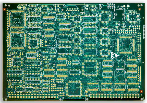
The gap between board design and the production floor
During the PCB design process, designers are limited only by the laws of electronics. In the real world, however, there are other limitations that come into play, such as equipment accuracy and material attributes. Simply put, DFM is the process of arranging PCB layout with the goal of making sure that it can be manufactured.
Let’s look at some examples to better understand this gap.
The first is annular rings. Annular rings are the copper pad area that is left after a hole is drilled through it. This ring is measured from the edge of the pad to the edge of the hole and is an important consideration in PCB design, as the plating on it allows an electrical connection to be made from one side of the hole to the other. In multilayer boards, annular rings have to align with sufficient overlap to allow that connection across layers. Perfect alignment exists on the drawing board, but even with the newest laser drills and high end machines, 100% accuracy does not exist. DFM ensures that annular ring width is great enough to allow for some misalignment between layers without breaking connections.
Another example is slivers. Slivers are narrow wedges of copper or solder mask that detach from the board during the manufacturing process and re-attach in a different location, creating a short. They can occur when a PCB layout contains very thin copper traces that are allowed by design rules, but in real life conditions have the potential to render numerous boards useless.
There are many benefits to DFM:
- Higher product quality
DFM decreases the number of design modifications needed to fit manufacturing equipment and processes, which can often compromise quality. - Shorter time-to-market
Product manufacturing is a long process with many opportunities for errors along the way. DFM helps reduce delays caused by scrapped products, errors, and time spent on revisions and documentation. It is important to note that design timelines may be longer, as every detail in the layout is reviewed to eliminate mistakes that could come up during production. It takes time to make the necessary changes, which can affect the timeline, but it reduces the time spent on costly iterations and fixing errors after production. In the long run, when looking at overall timelines from design to successful production, DFM pays off. - Reduced costs
DFM allows PCB designers to design boards for easy manufacturing, especially in mass production, while taking into account manufacturing guidelines and restrictions. When done properly, the result is a product that is easier and less expensive to manufacture. Cost reduction is also a result of higher yield rates, as there are less errors discovered in the manufacturing process. In fact, studies show that it can cost as much as 20% of the cost of the PCB for CAM engineering to prepare it for manufacturing.
DFM ensures a product can actually be manufactured in the first place by enabling companies to optimize all manufacturing functions while still in the design phase, as it includes all designs for bill of material (BOM) items and final assembly. This includes mold layouts, heat transfer analysis, tooling design and more.
Should you perform DFM if you are already performing DRC?
PCB designers often conduct Design Rule Checking (DRC). If DRC is already being performed, is there a need then for DFM? The short answer is a resounding yes. DRC and DFM are not the same, and both are needed for effective design and manufacturing.
DRC is an automated data analysis process that compares the entire design to baselines established by the foundry. Rules are used to define minimum physical requirements for PCB’s object, layers, nets, etc. which affects the board’s performance. The goal of DRC is to detect specific discrepancies or errors.
DFM on the other hand identifies production-related issues that could create manufacturing problems. When a DRC defect is overlooked, it will be found in every single copy of that board. A DFM issue, on the other hand, may manifest as a problem only on some boards, while others could perform perfectly.
So, is DRC enough? There are many things that would pass DRC and still cause issues down the line. We have already discussed slivers and annular rings. Other issues outside the scope of DRC include non-standard tolerances and materials, multiple surface finishes, unusual surface finish thickness requirements (particularly with gold), via plugging requirements, and many more.
In addition, DFM is often performed with a specific manufacturer’s capabilities and constraints in mind in order to assure better (cheaper/faster/more reliable) manufacturing. , DFM allows designers to pinpoint and fix issues during the layout stage, saving valuable time and resources down the line.
Getting it Done Right, DIY Style
DFM is nothing new. It has been around for years, typically performed by manufacturers. But as the demand for technology grows and evolves, so must the PCB designers. Designers need to extend themselves and take ownership of DFM in order to create not only great products, but timely and profitable ones. Online automated DFM tools allow PCB designers and layout engineers to validate their layout even before sending it out to manufacturers. PCB designers reclaim control over the product design, and eliminate inefficient back-and-forth between designers and manufacturers. Everybody wins: manufacturers receive more mature PCB layouts, fewer design spins are needed before a board can be printed, there is less scrap in productions, and products hit the market sooner.
Start validating your PCB layout today
You can start validating your PCB layouts easily with PCBflow, a free, online Design for Manufacturing tool that leverages market leading NPI software from Mentor and Valor. Simply upload your design to the secure cloud service that automatically checks your layout against nearly a thousand rules