Accelerate Design With Integrated FPGA-PCB I/O Co-Design
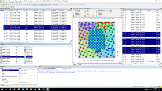
Did you know that a PCB design tool flow with FPGA I/O Optimizer technology eliminates the barriers between FPGA and PCB designers by accelerating design and providing a ‘correct-by-construction’ FPGA I/O assignment that supports pin swapping and layout-based I/O optimization within the PCB process?
Today more than ever leading-edge systems require a modern FPGA I/O optimization interface. In fact, the lack of, or poor FPGA I/O optimization often leads to longer routing cycles and longer trace lengths which in turn result in the need for additional signal layers and vias which can impact signal integrity and cost.
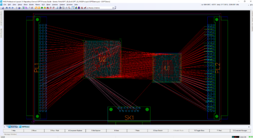
The ability to read in, export, and synchronize FPGA designers’ HDL and constraint files ensures full consistency during the iterative concurrent design process. Incidentally, it also allows creating high pin count FPGA PCB parts ready for instantiation in just minutes.
Modern FPGA I/O optimization not only helps you accelerate design time-to-market but also reduces manufacturing costs. To discover how you can create high pin count FPGA’s in minutes, enable collaboration between FPGA and PCB designers and how to optimize FPGA pin assignment in the context of the PCB layout – you want to check out our recent webinar entitled “How Integrated FPGA-PCB I/O Co-Design Accelerates PCB Design and Reduces Costs“. Now available on-demand!

To learn more about FPGA-PCB Co-Design Click here.


