ABCs of PCBs – N for Netlist
Welcome to ABCs of PCBs – a blog series to help new engineers learn about the world of Printed Circuit Boards. I’ll be covering topics from general engineering concepts to PCB design specific rules. As this is a ‘basics’ blog, I’ll keep the content software independent, but any visuals will be from the Mentor PADS Professional PCB suite.
If you missed the last post in this series: ABCs of PCBs – M for Manufacturing click here!
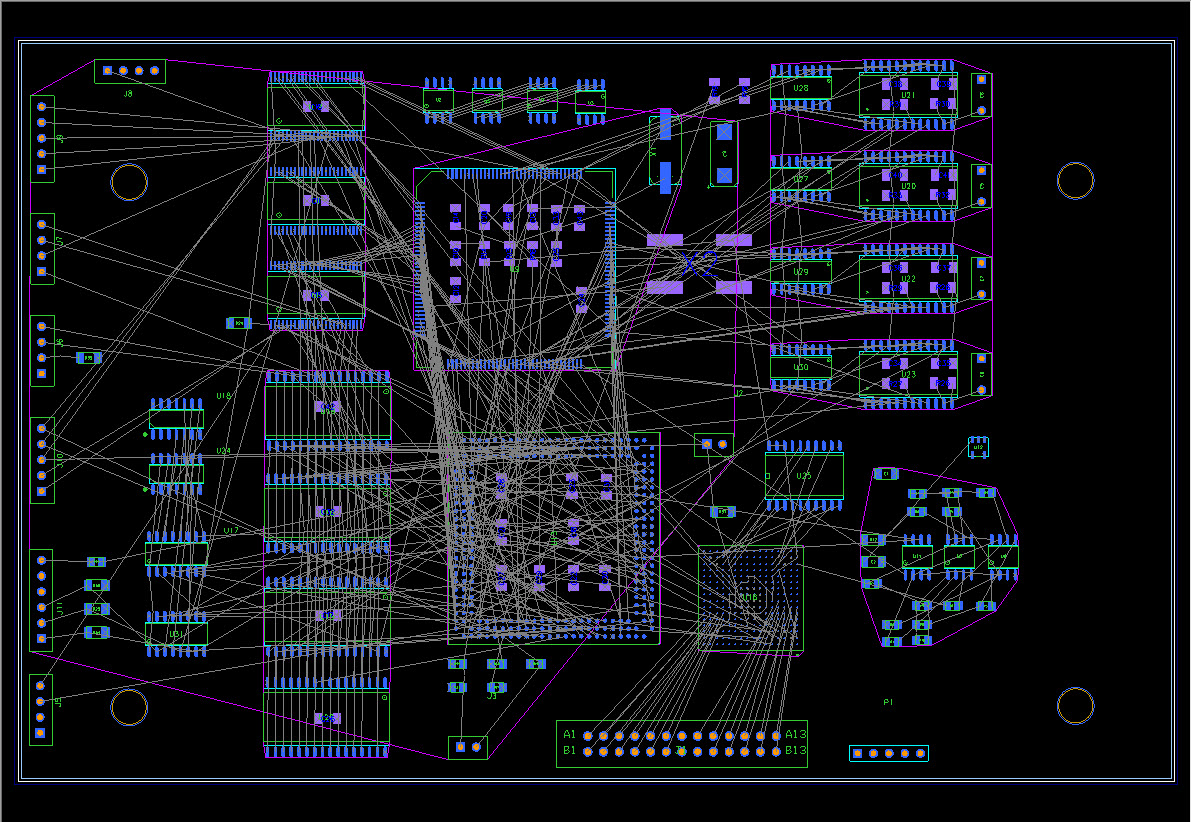
We’ve discussed quite a bit about tips and things to help make your PCB designs more accurate and efficient. This time, we’ll take a look at a vital part of the process itself – moving from schematic to layout. For most PCB design tools, you’ll find that you need to generate a netlist from your schematic and integrate it with your layout tool. Although this step usually happens behind the scenes of most full flow tools, it’s good to understand what this netlist entails.
Netlists store the most important net and connectivity information from your schematic to your layout. Imagine how long it would take for you to create connections, label nets, or assign pins in a schematic of your design and then have to recreate everything in a layout environment – how tedious! Netlists allow for the schematic aspect of the design tool to save information like reference designators, signal labels, pin assignments, and electrical connections. This translates into a PCB layout environment so that you are able to hit the ground running without any confusion or discrepancies of what was done in the schematic.
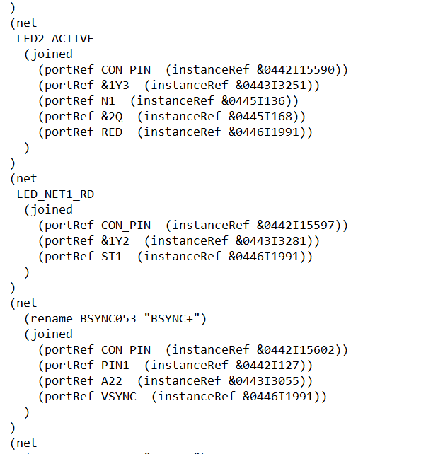
A netlist is a list of nets that define the conductivity interconnection scheme of a circuit board. Netlists do not contain trace data – they contain information about how the points should be connected, not how the points are connected. For example, “net_A connects to net_B” will be written in a netlist, but something like “net_A runs parallel to the bottom left of the board for 3in. before connecting to net_B” would not be expressed in that file.
For your designs in college, you may not need to review or edit a netlist file. But, as designs become more complex you may need to go back and change some of the netlist properties. One reason to make netlist edits would be if you need to adjust net names. If your schematic and layout tools are not integrated and do not sync in recognizing name formats, you’ll need to make changes in order for a clean transition. For example, if your schematic software acknowledges dash marks (net-A), but your layout tool does not, it’s important to edit the netlist to fit the tool’s format (changing ‘net-A’ to ‘net_A’).
If you’re using a full flow PCB system – one that has the ability to create a schematic and go straight into layout – you may never need to go into a netlist file. Regardless, it’s always important to understand the basics of what’s happening behind the scenes. Export a netlist from your own design and take a moment to see what it entails!
Are you a student? If so, try your hand at designing and testing a PCB with the free PADS Professional Student Edition.
Thanks for reading and see you next time for more on the ABCs of PCBs.
-Shivani Joshi


