ABCs of PCBs – I is for I (Current)
Welcome to ABCs of PCBs – a blog series to help new engineers learn about the world of Printed Circuit Boards. I’ll be covering topics from general engineering concepts to PCB design specific rules. As this is a ‘basics’ blog, I’ll keep the content software independent, but any visuals will be from the Mentor PADS Professional PCB suite.
If you missed the last post in this series: ABCs of PCBs – H for Hierarchy click here!
You probably learned about the letter ‘I’ in kindergarten. Somewhere along the way, you learned that ‘I’ was a homonym for ‘eye’. Then, if you took physics in high school, you learn about a different meaning for the letter ‘I’ – current. *Fun fact: ‘I’ stands for intensity – as in the intensity of current or electrons*
‘I’ is a fundamental component of electronics. You’ve probably learned what it is, many different ways to calculate it, and its effect on your designs. Now, it’s time to apply what you’re learning to the world of PCBs.
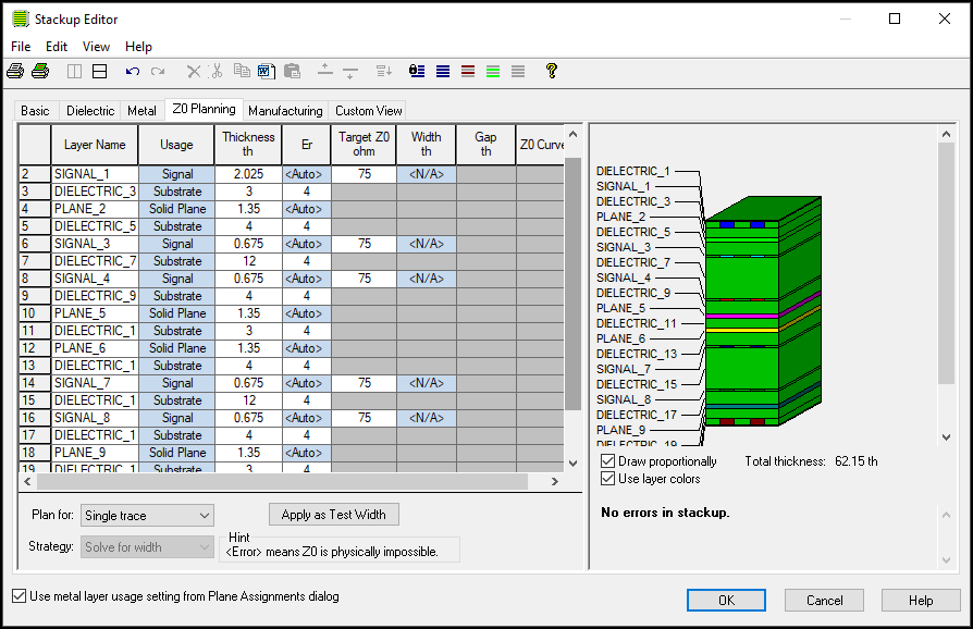
When the board is ready to go and connected as its final product, you will have current running through it – but what if you have too much? Or too little? Analyzing current flow and current density are important steps to take before producing a board.
Just as a wire carries current from point A to point B, a trace on a board delivers current. We can simulate current in most design software to make sure we are meeting our project requirement. However, current density is often overlooked. Current density is defined by the amount of current flowing through a conductive area. J = I/A where J is current density, I is current, and A is a cross sectional area. This can typically be adjusted at the stackup level.
When designing your board, you’ll want to take into account a few things to make sure you’re handling the current properly:
Trace width
We all know the equation V = I*R. Now, imagine you have a set voltage and current for a trace in your design; so now the only variable you have control over is resistance. In the PCB world, this translates as a variable in trace width. Just like wires, the smaller the trace, the more impedance you’ll face. If you are running a high voltage trace, it’s typically a good idea to increase the width, therefore lowering resistance. There are many trace width calculators online that can help you solve for the minimum required width for your different traces.
Temperature
If you’re an electrical engineering student, thermal properties might not be something you tend to focus on, but it’s a habit definitely worth changing. The traces on your boards will generate heat because of power dissipation. P = I2 R. We’ve talked about the damage heat can do on your PCBs, so it’s always a good idea to do a quick analysis, if you can, or adjust your current density accordingly. Reviewing datasheets of components like ICs is a great practice to follow in order to make sure you’re following their operating parameters.
The more you research, design, and practice, the more you’ll learn about what to look out for. Current can be tricky, but with the proper analysis at the design phase, you’ll be sure to produce some great boards.
Thanks for reading and see you next time for more on the ABCs of PCBs.
-Shivani Joshi


