ABCs of PCBs – G for Ground Planes
Welcome to ABCs of PCBs – a blog series to help new engineers learn about the world of Printed Circuit Boards. I’ll be covering topics from general engineering concepts to PCB design specific rules. As this is a ‘basics’ blog, I’ll keep the content software independent, but any visuals will be from the Mentor PADS Professional PCB suite.
If you missed the last post in this series: ABCs of PCBs – F for Flexible Circuit Design click here!
A ground plane, in the PCB world, is a layer or large area of metal connected to ground. Though ground planes aren’t always critical to creating a board, they are preferable. They not only enhance design performance and help in avoiding some design issues, they serve as the return path for current from many different components.
I had first mentioned the benefits of adding a ground plane in B for Board Layout and now it’s time to dive deeper into the benefits of this technique. You should always be looking for ways to improve your designs signal integrity to reduce electrical noise and interference. This includes suppressing crosstalk and EMI (electromagnetic interference), both of which can be accomplished with proper grounding practices.
EMI can be reduced by routing return traces next to signal traces, especially when high speed designs are involved. As helpful as this method is, it’s not always realistic to add these return traces due to limited space on the board. When suitable, adding a ground plane can also address the goal of limiting EMI with close ground return paths.
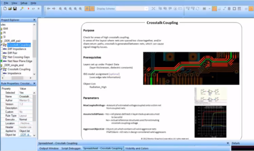
Crosstalk is another common issue we see when creating PCBs. One way to avoid this is by using a ground plane between two signal layers. This grounding practice creates distance between these active layers and provides a cleaner return path. This added ground plane results in diminished crosstalk.
If this is your first time designing a board, you may be working on a 2 layer PCB. Since creating a ground plane as a whole layer is not possible, you should consider using filled areas or flooding the external layer(s) after routing. Using a hatch pattern on external layers for large PCBs helps to ensue copper adheres to the PCB and avoids board warpage.
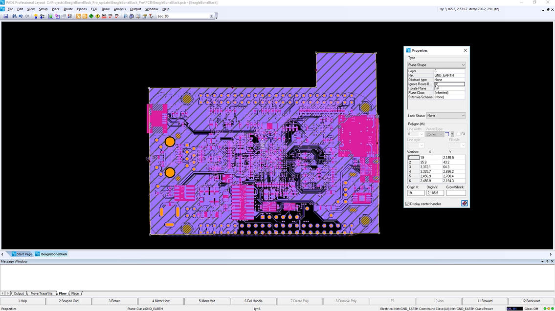
Flooded ground shapes on external layers can also be connected to internal ground planes easily with stitching vias. These connections give you a little more simplicity when routing the PCB since you are able to connect directly which frees-up PCB real estate for signal routing. Easier access to a ground plane also lowers the frequency of ground loops since components connecting to ground can access GND directly. You’re likely to see that 4 layer PCBs include a ground plane due to these major benefits. Multi-layer PCB’s on th other hand – may have several throughout the entire PCB stack-up.
Thanks for reading and see you next time for more on the ABCs of PCBs.
-Shivani Joshi