Layout automation using advanced PCB design techniques – Part 4
In part 3 of this blog series we looked at what typically is the longest stage in designing a PCB Routing and net tuning. In part 4 we will finish the design process by looking at planes, and some miscellaneous items that may be required in some designs.
Planes
Typically one of the last major tasks to complete a board design aside from documentation is creating plane areas. Many of today’s designs include 10, 20, 30+ plane areas or very complex board outlines. All of which can consume a good portion of our design time. One type of circuit design that requires special attention is power supplies. We need to keep inductance down and create copper areas that can handle high current. Doing this with traces is not the best option. Using planes and solid connections to pins is the simplest method. Drawing simple rectangles and circles, using merge and cut commands, full shape corner manipulation, and setting per shape plane thermals, allows us to create complex plane areas in seconds to minutes, not minutes to hours.
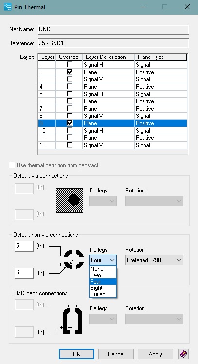
Additionally when dealing with through hole pins in power sections, it’s far less time consuming to modify pin thermal settings based on layer and usage rather than at the library level giving us unlimited flexibility, Figure 8.
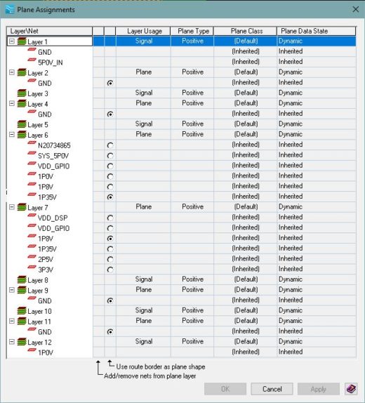
I mentioned complex board outlines. We can now create full board area planes in seconds by taking advantage of this shape and not having to replicate it. Having one central location to control what nets are assigned to a layer, which net is allowed to use the route border as its plane shape, and setting the state of the shape facilitates proper design management Figure 9
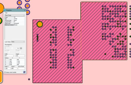
Working with a 4 or 40 layer board, at some point we need to create embedded planes. As I showed earlier, using simple rectangles and circles instead of drawing complex polygons dramatically reduces the time it takes to create embedded planes. Let’s go through 2 examples. First we’ll create an embedded plane using rectangles and merging of shapes. What’s the advantage of taking the time to merge shapes? It allows us to easily move the shape at any point and change properties. Next we’ll create the same shape using rectangles and merging/subtracting of shapes. Having this option gives us flexibility as each design possess different challenges. To finish off our plane area we’ll round all the corners. PADS Professional provides options like this that makes performing shape manipulation less painful than most tools, Figure 10.
Download a free trial of PADS Professional today!
If you’ve been designing PCB’s for some time at some point you’ve had to fill a plane area with vias or place guard vias around a trace. When placing one by one this takes forever. We have a requirement with our design to create a ground plane directly under our RJ-45 connector and fill with vias. Using stitch shape we can play with several scenarios and choose the most appropriate as it only takes a few seconds to process. In case we create more plane areas requiring via fill, we’ll save this configuration. Later when creating a shape we can than assign this configuration, Figure 11.
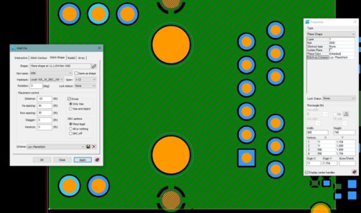
Now that we’ve saved a configuration, if we undo our via stitching we can assign our new via stitching configuration. To perform the stitching process, we simple select and right-click over the shape and choose Generate Stitching Vias. In a few seconds our job is done.
Miscellaneous
Teardrops
Teardrops are not always needed but when we have to use them it should not be a cumbersome task. Being able to control the length and width is mandatory otherwise some designs may require adjusting far too many traces to make sure teardrops can be added without creating DRC errors. In our BGA area we can window select traces requiring teardrops, right-click and choose Teardrop. If the entire design needs teardrops simple set an option for all pads Figure 12.

As a specialized function we can fine tune teardrops by setting curved settings for areas where space is at a premium. Notice how the copper being added is not uniform between each side but fills in as needed to make a con-formal curve.
Interactive Design rules
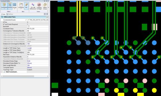
There may be times when we want to make quick adjustments to an electrical constraint. Let’s say we forgot to define a differential pair. With PADS Professionals Constraint Editor add-in window in both the schematic and layout tools we can quickly adjust electrical constraints and define a differential pair, Figure 13. Trace matching and length data can be viewed based on your selection as well.
DRC Visualizer
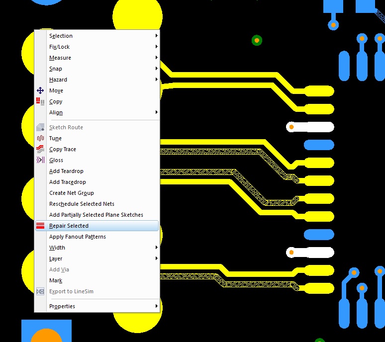
We’ve now been notified by our engineering lead of a change to the 100 ohm differential pairs and space requirements. We could rip up the traces and reroute, but to fix we’ll just change the trace width and then let the tool do the rest by using Professionals DRC Visualizer and Repair Selected Figure 14.
In Closing
To recap what we’ve talked about. Several new technologies exist that can dramatically impact the time required to design a PCB. The core part of PCB design, component placement, routing, and plane creation can all be made simpler and take less time using the following advanced automation available in PADS Professional; Design rules, Sketch routing, Auto-tuning, Plane creation.