Why and How: Hierarchy vs. Flat PCB Design
Organizing a schematic of a PCB can be done in many ways – using different sheets for each function of a design or adding labels and comments for each segment – all with key benefits to the PCB design process. Here, let’s focus on the organizational tactic: Hierarchy.
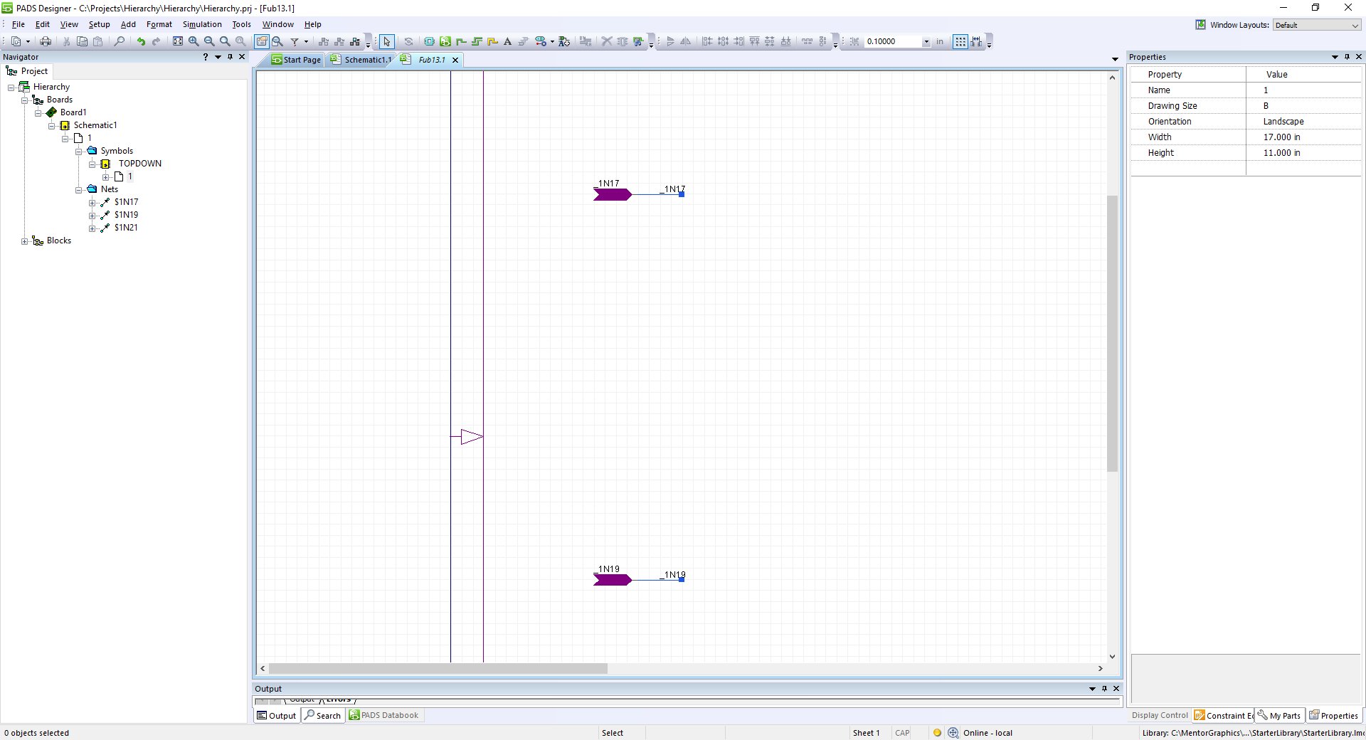
In the PCB schematic world, hierarchical design is a practice in which grouped segments of a design are represented by block symbols. This is sometimes referred to as block design. Hierarchy is not always necessary, but comes with some major advantages:
Reuse of schematic designs
After creating a block with a segment of the design, you can save the block to use later in other areas of your project and even in different projects. This allows for a standardization among designs.
Concurrent engineering
Allowing for a design to be broken into different blocks gives engineers the flexibility to designate each block to a different specialist or team. Instead of passing around a design, each segment can be created independently and organized at a later time.
Troubleshooting
When there’s an issue with one area of the design, engineers can work within a block to find the solution. At the same time, if the issue may lie outside a block, there’s less circuitry to shuffle through.
There are two methods of creating hierarchy: Bottom Up and Top Down.
Bottom Up
- Create lower-level schematic with ports for input and output
 2. Create a composite symbol
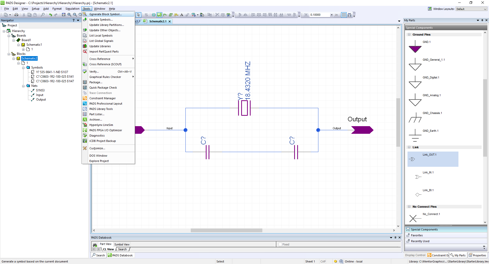
3. Place in top-level schematic
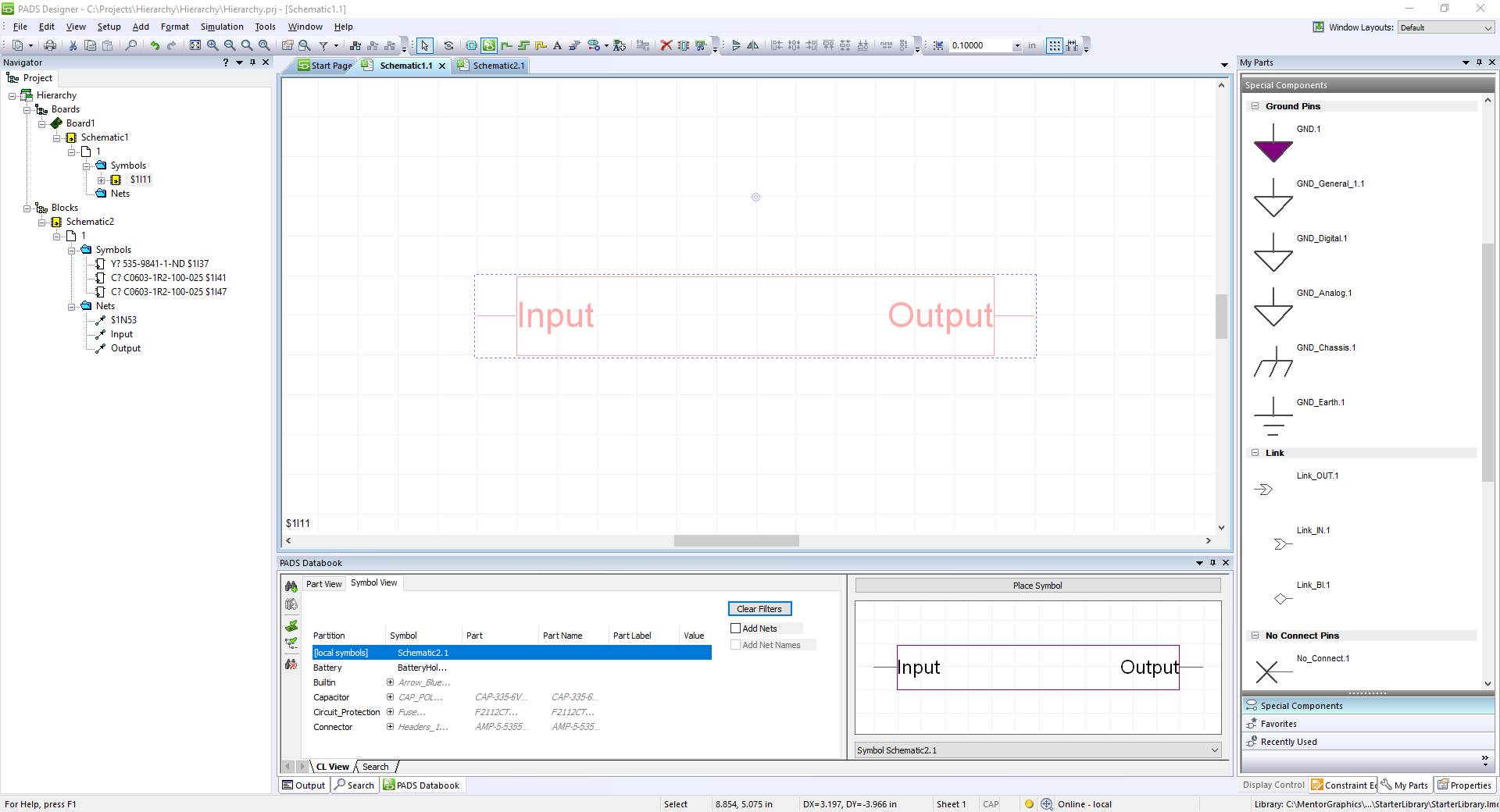
Top Down
- Create a block in top-level schematic
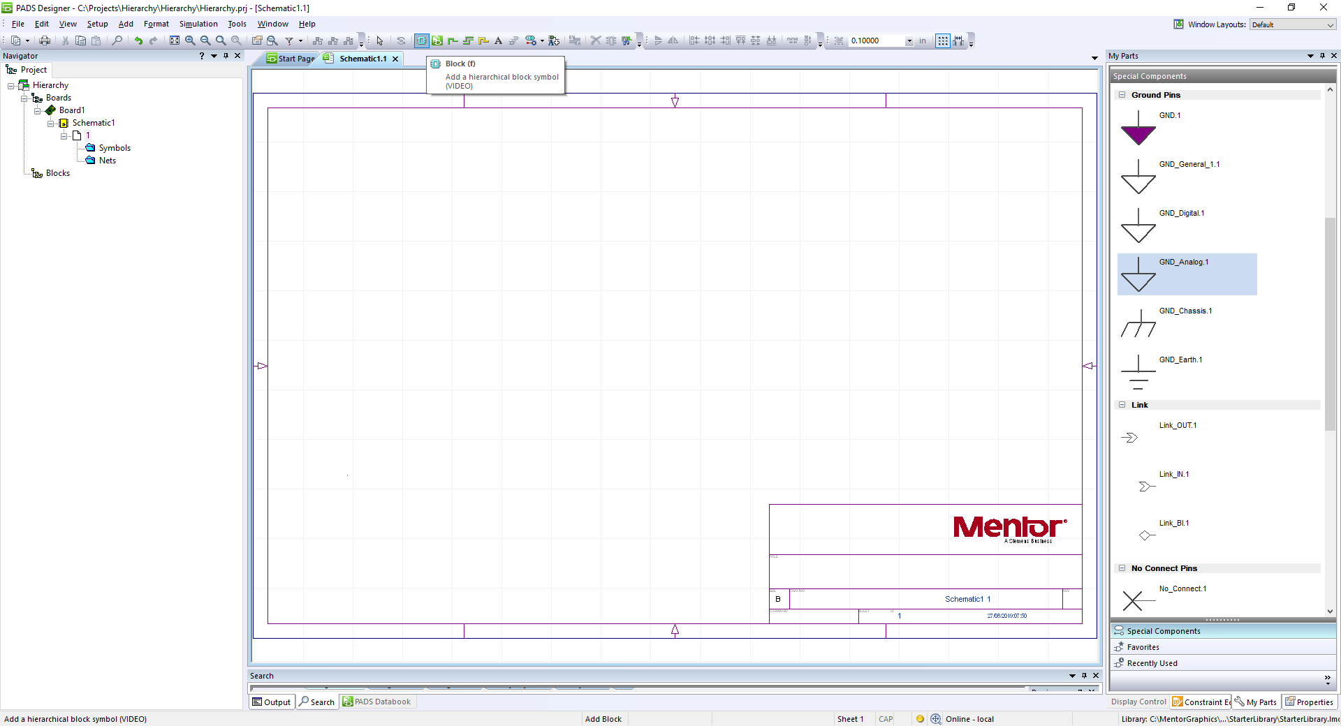
2. Add connectivity to the block

3. Push into block to create lower-level schematic in block
Each method has produces the same end product – it all comes down to preference. Typically, Bottom Up thinkers like to plan out and design every step of the way while Top Down thinkers like to conceptualize the entire project before diving into designing each block.
If you want to learn more about creating hierarchy in your schematics and overcoming other challenges in your design process, check out this webinar!
Thanks for reading!