What is the best method for PCB component placement?
Component placement is that process that is started shortly after you have created your schematic, and you are now looking to start designing the physical PCB. Good component placement on is crucial to a PCB design, and optimal location of the components on a board can be effected in various ways. For instance, placement of a device can be determined by another object on or near the board in the overall design. Also, during placement it may be required that certain components need to be placed within a certain proximity of one another for routing or thermal purposes.
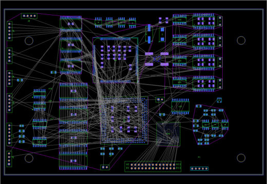
There are many PCB tools out there, and they all go about component placement in similar yet different ways. One of the more common ways I have seen, is for the components in the design to be placed in the drafting area, dispersed around the board outline of the PCB being created. While this method is not bad, on a board with hundreds of components this method can tend to get messy.
The best method for placing components, would be to have them in a “bucket” where you can pull them out and on to the board in any order you want to place them. An even better way would be to have the ability to group these components, either in the schematic or as the board is being laid out, so you can pull sets of components that need to be placed close together out at the same time.
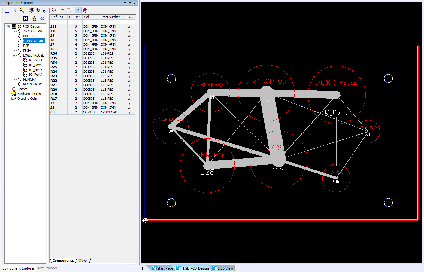
This last method I described is exactly how PADS Professional operates when placing components on your board. The Component Explorer is the “bucket” that holds all of the components in your design until you are ready to place them in either 2D or 3D. Users can create in either the schematic, or in layout, placement groups of components that need to be located near each other. These groups when placed are shown as circles, and the size of the circle represents the approximate board space the components in that group will take up. Also, as these groups are placed, the connectivity between the groups is shown as netlines of varying sizes, the larger the netline the more connectivity between groups.
If you want to learn more about component placement, including group placement planning, check out this webinar. It also goes over component placement, as well as some other helpful information about the advanced features of PADS Professional.


