Designing PCB’s for IoT – Part 4: Schematic and Layout
This is Part 4 in a blog series examining the unique aspects of IoT PCB design. Click here to read Part 1: IoT Everywhere. Click here to read Part 2: IoT Design Domains and Click here to read Part 3: IoT Design Form, Fit and Function
In part 3 of this blog series I discussed how an IoT product’s form, fit, and function are critical to its success. Now let’s take a look at specific features and functionality in schematic and PCB layout tools that help support the electronic design challenges associated with the different IoT design domains.
Capturing the IoT Design Intent in the Schematic Diagram
Once the IoT component selections are made and symbol library creation is complete, the next step is to define connections between the components in a schematic diagram. To achieve design efficiency and 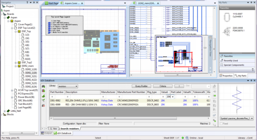 productivity, schematic creation should include component management to source components and manage costs. Direct access to analog/mixed-signal circuit analysis and pre-layout signal integrity analysis from within the schematic design environment is critical to ensure that the design’s signal integrity and physical characteristic requirements are achieved. A properly captured rules-driven schematic ensures that constraints are driven into the PCB layout.
PCB Layout of IoT Designs
IoT designs, especially for consumer products like wearable devices, are driven by a pre-defined, marketable form factor that is typically designed within a mechanical CAD tool. Being able to see the board with components placed in its enclosure in 3D prior to routing traces or pouring planes is essential for ensuring that the design will meet all of the product’s physical requirements.
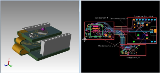
In addition to the PCB outline, other factors, including the product’s use environment and flexibility, must be taken into consideration. These factors include component placement, constraint management, ECAD-MCAD collaboration, support for rigid-flex circuits, and assurance that the design can be manufactured cost effectively and is testable.
In parts 1 and 2 of this blog series we began to realize the broad uses and demand for IoT technology in electronic products. In Part 3, we explored the importance of the “3-F’s” for IoT product creation. And here, in Part 4, we took a look at specific schematic and PCB layout tool features and functionality that help with IoT design. Coming up next in Part 5 of this IoT blog series, we’ll take a look at the manufacturing and assembly for IoT Designs.
To learn more about the schematic and layout tool capabilities needed for IoT design download my white paper: 7 Design Aspects of IoT PCB Designs.
Thanks for reading!
John