Designing PCB’s for IoT – Part 3: IoT Design Form, Fit and Function
This is Part 3 in a blog series examining the unique aspects of IoT PCB design. Click here to read Part 1: IoT Everywhere. Click here to read Part 2: IoT Design Domains
In part 2 of this blog series I discussed some the complexities of IoT designs specifically regarding mixed-technology design domains. IoT product PCBs can be quite complex and they must be prototyped to ensure that the technology works as designed. You’ll need to know whether all of the required components meet the product’s form, fit, and function requirements or, perhaps, whether you’ll need to invest in a custom chip design that consolidates components.
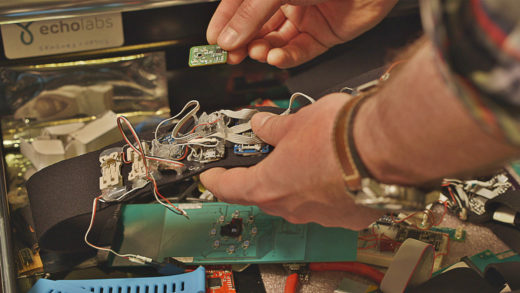
Fig. 1 – Prototype of biomedical wearable wristband developed by Echo Labs (photo via Echo Labs)
A key driving requirement for the design of many mass-consumer IoT devices, particularly those with a human interface, are the form, fit, and function. These “3-F’s” for IoT design are not the typical “3-F’s” of engineering.
- Form – Size matters. In fact, the shape and appearance of the product, including its weight, size, color, density, orientation, and dimensions all matter. If a fitness tracker is not lightweight, comfortable, or even fashionable, or if a smart watch is too bulky, or an IoT door lockset doesn’t fit in aesthetically, the product may very well never get off the ground.
- Fit – The fit of the product in the market, the price point, the timing, and the competitive landscape can all be deal breakers in the fast-paced market of IoT products. Even a great idea that can’t be produced economically or is overpriced may never take off. Consider VR (virtually reality) headsets. They have been around for decades. Original units costs 10’s of thousands of dollars, were hardwired to machines, and were unheard of as a consumer product. VR headsets today are wireless and mass produced. High-end VR units can now be purchased for less than $500.
- Function – Most simply, it’s what the product is meant to do. Does it solve a problem? Perhaps it’s a new product category altogether. In Fig. 2 below, you can see the evolution of this device from its prototype stage (Fig. 1), to a consumer wearable product. This tracker utilizes optical sensors and spectrometry to measure and analyze blood composition and flow. It also monitors heart rate, blood pressure, respiratory rate, and full blood gas panels.
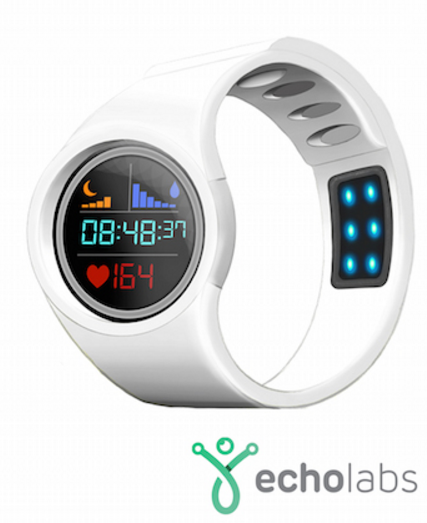
Fig. 2 – Biomedical wearable developed by Echo Labs (image via Echo Labs)
In parts 1 and 2 of this blog series we begin to realize the broad uses and demand for IoT technology in electronic products. We have also identified some of the complexities of designing in the mixed-technology domain of IoT. And in this blog we’ve explored the importance of the 3-F’s for IoT product creation. In Part 4 we’ll be taking a look at specific schematic and PCB layout tool features and functionality that help support the electronic design challenges associated with IoT design.
To learn more, download my white paper: 7 Design Aspects of IoT PCB Designs.
Thanks for reading!
John


