The PCB Design Ecosystem
In printed circuit board (pcb) design, a product creation ecosystem enables engineers to address the nuances of design early and throughout the technology development cycle. From component selection to manufacturing output, a robust, scalable and unified pcb design tool is needed to meet critical performance, schedule deadlines and cost challenges.
Yes, today’s high-tech products are faster, smaller, and smarter than ever and the time-to-market demands to deliver high-quality products that are competitive, cheaper and faster means that design tools must be able to consider every aspect of the design throughout a product’s creation, from functional specification to end-product performance. And with IoT, Bluetooth, WiFi, and RF technologies everywhere, design concerns related to mixed signals, power consumption and thermal analysis must be measured and addressed throughout every stage of the design, from the component level through to final assembly.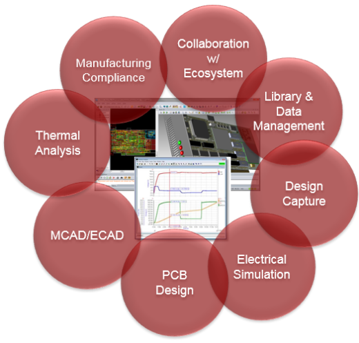
Product Creation -Tool Requirements
This short excerpt from my recent article published in EP&T – Electronics Products and Technology, read the full article here: http://www.ept.ca/wp-content/uploads/sites/29/2016/05/EPT2016May01downloadable-1.pdf highlights how access to design IP and collaboration is key to meeting the needs of engineers in electronics product design in today’s PCB design ecosystem.
Learn more about the PADS Product Creation Platform
Thanks for reading, John