Why impose PCB design constraints? Part 3
This is the third in a three part series examining rule and constraint definition and management that supports a correct-by-design methodology.
In my earlier posts in this series (first and second), I discussed our need to achieve compliance to design rules versus constraining our designs. I also highlighted the importance of rule definition and management and then did an in-depth review of the rules and constraints that are needed to meet our design and system performance goals and manufacturing quality targets. In this post, I review the need for proper planning of rules and constraints.
Constraint Planning
I’ve discussed the different types of constraints and the importance of ease of use in their set up, so now let’s take a look at planning. Constraint planning and definition can and should take place as soon as the design project is created. Reuse constraints from a previous project(s), use a predefined template of rules, or create them specifically for your new design.
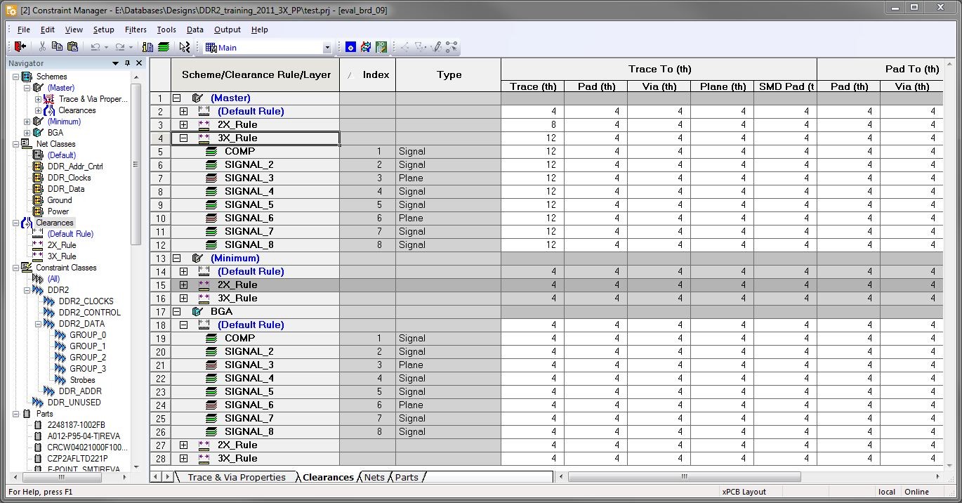
Reusing existing rules or a template ensures that any common constraints, such as those for DDRx and PCI-E busses, differential pair rules, and manufacturing requirements are adhered to. It also minimizes the possibility of input errors.
Proper grouping and definition of net classes and constraint classes in the early stages of the design process simplifies constraint definition and management significantly. Grouped constraints can increase layout efficiency, reducing design time and, ultimately, lower PCB design costs.
Net classes are used to organize and speed the definition of routing constraints for nets with similar characteristics. For a net class you can define the layers allowed for routing, the corresponding trace-width range for these layers, and the via types allowed for nets in the net class. For differential pairs, you can define a layer-dependent differential pair gap.
Constraint classes are used to organize and speed the definition of length, topology, and other constraints for nets with similar electrical and timing properties. Although constraints assigned to a constraint class may be applied automatically to all nets in the class, particular constraint values can be customized for individual nets, pin pairs, and differential pairs.
Summary
In the first of this series I mentioned that all we are trying to do when defining rules and constraints is “to achieve compliance (conform to all of our system specifications and rules for high speed performance, manufacturing, power distribution, heat dissipation etc.).”
In order to achieve that compliance, we need an integrated constraint definition and management system that is available throughout the design flow, is easy to use, supports re-use and templates, and is consistent, efficient and accurate, which should validate required versus actual measured (PCB routed) values.
That’s really not a lot to ask for, right?
So, in finishing, I have the same question as before for you – what is the most challenging aspect of design rule/constraint entry and management that you face today? Are there new and upcoming technological requirements that are difficult to address?
To learn more about the importance of PCB design constraints, check out this white paper, Why PCB Design Constraints Should Drive Your Design Flow.