Why impose PCB design constraints? Part 2
This is the second in a three-part series examining rule and constraint definition and management that supports a correct-by-design methodology.
In my first post in this series, I discussed our need to achieve compliance to design rules versus constraining our designs and the importance of rule definition and management. This time I would like to take a closer some of the rules and constraints that are needed to meet our design and system performance goals and manufacturing quality targets.
Rules and constraints
Typically when we discuss the topic of constraints, in relation to our PCB designs, we often assume that we are referring to the high speed routing rules. Of course, there are a myriad of electrical based rules that we do need to consider, including:
- Clock signals
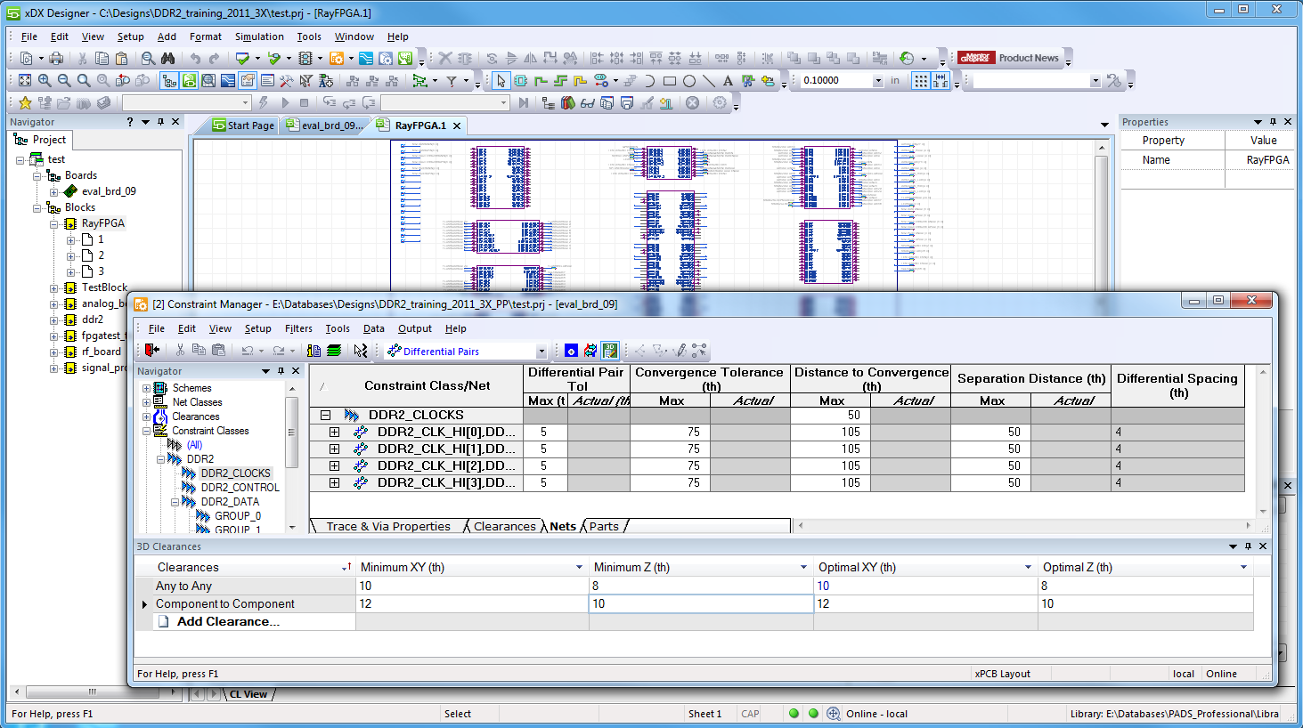
- Differential Pairs (convergence tolerance, separation distance etc.)
- Bus structures such as DDR3/4 and PCI-x etc.
- Net Topologies (MST, Daisy Chain, Tree etc.)
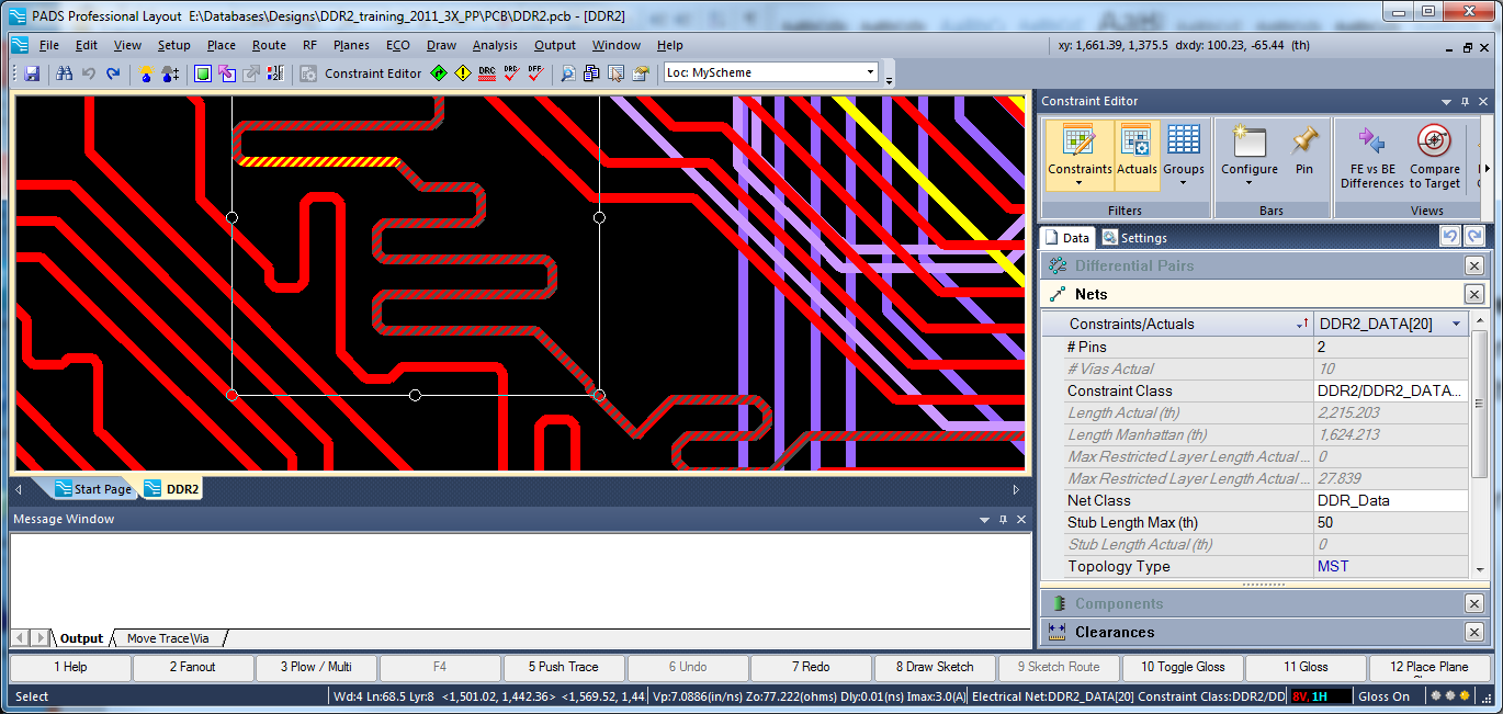
- Delay and impedance matching
- Net Classes and Constraint Classes
- Other critical circuits and nets
Additionally there are many other physical based rules and constraints that also need to be considered. These include:
- Trace widths and clearances
- Copper spacing (plane shapes, component pads and other board objects)
- Solder mask and silkscreen layer data
- Contours, mounting holes, non-plated versus plated holes
- Component clearances (between components, and board edge etc.)
- Z axis clearances (shadow clearances)
- Logical component groupings (to define and aid placement planning)
- 3D clearance checking
- Layer stack-up definition
In order to effectively define and manage all of the rules and constraints we impose on our designs, there clearly needs to be an integrated environment that is easy to use (intuitive) and available throughout the complete design flow.
After all, independent engineers who are responsible for the entire design should not have to enter rules at the schematic and later have to either reenter them at the PCB layout stage or use a different tool to modify them.
Interactive and online DRC settings which are adhered to throughout the design cycle provide for an error free (correct-by-construction) design when carefully planned early in the design phase.
Constraint editing during PCB layout provides several benefits including the opportunity to compare the actual routed values versus the defined rules. It is also useful to be able to limit the view of the design constraints to just those you are specifically focused on at any given point in the layout such as routing your clock signals or differential pairs.
More on this topic in the final post. In the meantime, I have the same question as before for you – what is the most challenging aspect of design rule/constraint entry and management that you face today? Are there new and upcoming technological requirements that are difficult to address?
To learn more about the importance of PCB design constraints, check out this white paper: Why PCB Design Constraints Should Drive Your Design Flow.