Can Your Verified PCB Design Fail in the Lab (or in the Field)?
 Design verification is typically performed before building the design prototype or manufacturing the design. These checks are performed either manually or using the DRCs built into PCB layout tools. Manual checks are performed by printing each layer of the stackup and visually inspecting them using a loupe. As you can imagine, this approach is prone to errors, is time consuming, and is generally performed by the more experienced PCB designers on the team.
On the other hand, DRCs that are built into layout tools are automated, can be run iteratively in the design cycle, and find all the design issues that the DRCs are built to find. While a few layout tool DRCs have access to a field solver, none have access to a geometry engine to perform electrical checks. Layout tool DRCs have limited scope. They are used to improve design manufacturability, but they come up short when checking a design for electrical issues, such as the distance between the IC power pin and decoupling capacitors.
How often has your design passed manual or layout-tool DRC inspection, but failed in the lab?
What if you could increase the scope of your post-layout design verification ? Enter HyperLynx DRC.
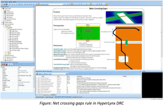
A design and electrical rule check tool such as HyperLynx DRC contains signal integrity (SI), power integrity (PI), and EMI/EMC checks. Such checks are not performed by layout tool DRCs because layout DRCs are primarily built to measure distances between design objects such as trace segments. For example, the nets crossing gaps rule (see Figure) utilizes a complex geometry engine to look for signal nets that experience impedance discontinuities (that cause SI issues) and generate electromagnetic fields that cause EMI/EMC issues. HyperLynx DRC’s comprehensive suite of EMI/EMC-related checks (included in higher tiers) additionally includes IO coupling, exposed length, edge shield, and vertical reference plane change.
With HyperLynx DRC you can:
- Identify design issues that existing design verification approaches may not (or are not built to) find
- Expand the scope/coverage of your PCB design verification to include SI, PI, EMI/EMC checks.
- View/inspect your PCB layout outside the confines of the layout tool
- Save and distribute rule parameters to perform design verification earlier in the PCB design process (think: cheaper to implement fixes)
- Alleviate pressure on the most experienced individual(s)
- Mitigate process bottlenecks.
Lessen the risk of design failures by incorporating HyperLynx DRC into your PCB verification process – for free! Get more information.


Comments
Leave a Reply
You must be logged in to post a comment.
its good