DDR Design: Write leveling for better DQ timing
 So far, we’ve gone through the basics of the DDR Bus, and discussed some of the Signal Integrity and timing requirements of the controller and the DRAMs.
Let’s now dig down into one of these timing requirements, specifically the clock-to-DQS requirement at the DRAM and the industry-standard solution of “write-leveling” used to solve the layout issues caused by the requirement.
Understanding the clock-to-DQS requirement
First, let’s start with the basic requirement. There are three official requirement variables with extremely ogre-ish names – tDQSS, tDSS and tDSH. Rather than discuss the details of what these imply (I guarantee you’ll forget them 90 seconds after reading them), let’s talk about the conceptual idea behind the requirements.
These three variables provide a way of specifying that when the clock and strobe reach the DRAM, their rising edges occur within a certain time-span of each other (often around ±tCK/4).
For a single DRAM setup, this isn’t a problem. If the clock and strobe signals are reasonably length-matched, then the clock and the strobe will arrive at the DRAM at approximately the same time.
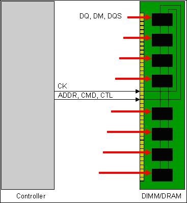
For DDR2 and earlier technologies, this again isn’t a problem even though they had multiple DRAMs. In these setups, the clock to each DRAM was length-matched to each other by means of a tree topology. So, if there were eight DRAMs in the channel, the clock lengths from the controller to each of the DRAMs was matched to be equal to the strobe length to the DRAMs.
Problems appear as speeds get higher
A tree topology, however, is full of reflection segments. Each branch creates a discontinuity, not to mention that there are multiple endpoints. As the data rates get higher, managing Tree topologies becomes more difficult.
For DDR3, the solution was to use “Fly-By” routing. With this routing, the clock (and address) signals start at the controller and create a main channel to all the DRAMs. The DRAMs are connected to the main path by means of a very short stub from the main routed signal. This way, stubs are minimized and the main path can be terminated neatly at the end of the route.
However, this creates a fundamental problem with respect to the clock-to-DQS requirement at the DRAM. With fly-by routing, the DRAM closest to the controller will receive the clock and address signals before the DRAM at the end of the routing. So, the data and strobe needs to arrive at the first DRAM earlier than at the last DRAM in order to line up the clock and strobe. Shortening one lane and lengthening the other won’t work since this will cause an issue during read transactions.
Solving the problem
The solution is for the controller to automatically detect the flight-time difference of the clock signal between the different DRAMs, and then delay the data lanes appropriately so that they reach the DRAMs as the clock/address signals reach the DRAMs. The process of detecting the required delays, which is usually done at power up, is called “training.” The entire system is called “write leveling.”
It is similarly possible to delay each DQ bit within a lane with respect to its strobe in order to perfectly center the strobe around the DQ signal. This feature is available more commonly in DDR4 controllers and in some of the higher-end DDR3 controllers. It is known by many names, including “per-bit leveling,” “DQ calibration,” or “DQ-DQS deskew” (say that 10 times fast!).
For more information about the physical design issues of high-speed interfaces, read our white paper.


