Innovations in physical verification tools and technologies keep the IC industry moving forward
By John Ferguson
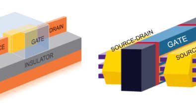
A few years ago, I was invited to present a paper discussing the advances in physical verification and cloud computing, and how they have helped the IC industry continue moving forward despite the mounting challenges to Moore’s Law. The opportunity to stop and think about how we got HERE from THERE made me realize just how much unnoticed innovation is constantly occurring in the EDA industry. Some of the changes in IC design produced verification challenges of their own, such as the use of finFET and gate-all-around finFET transistors, which present questions of performance, scalability, and variation resilience. Others, such as multi-patterning, were introduced several nodes ago as temporary stop-gaps, but now show no signs of going away, despite the introduction of extreme ultraviolet (EUV) lithography technology that was supposed to herald their demise. Some, like fill, have evolved from a simple DFM process to a critical success factor, with nearly infinite variations requiring complex analysis to determine optimal shapes and configurations.
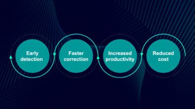
And how did the EDA industry respond to these changes? Not surprisingly, much as it always has. EDA companies have always had to evaluate and experiment with leading-edge IC design and manufacturing information to assess the impact of changing technology on design verification and optimization. With the knowledge they gain through collaboration with both design companies and foundries, they develop and implement new functionality and new tools that reduce or eliminate verification time and resource impacts while still ensuring accuracy and full coverage. Constantly replacing inefficient, less precise verification processes and tools with smarter, more accurate, faster, more efficient, and more automated functionality helps the IC industry maintain, and even grow, both the bottom line and product quality in the face of increasing technological complexity.
Joe Sawicki, the executive vice president of Siemens EDA, is fond of saying that Calibre tools break at almost every node in some big fundamental way, and we rewrite the underlying code at every node in some big fundamental way. That rewrite, while rarely visible to end users, is what enables the performance, accuracy, and ease of use of the Calibre toolset to constantly improve while also absorbing new design styles, increased complexity, and ever more demanding market requirements.
Beyond this improvement of the IC verification process itself, the introduction of new technology, such as cloud computing, provides a new and unique opportunity to accelerate the time to market for designs. When you consider the growth in computing requirements at advanced nodes, it’s not hard to understand why tapeouts are taking longer and requiring far more resources. By removing cost and latency barriers to resource usage, implementations such as EDA cloud computing allows companies to obtain instant access to the CPU resources needed to achieve their physical verification turnaround time goals (e.g., overnight runtimes), even in the face of the exponential compute growth at the newest technology nodes. Having access to EDA technology in the cloud can also provide a fast, cost-effective means of dealing with emergent situations in which all internal resources are committed, but a critical issue requiring immediate resolution arises.
To learn more about how Calibre Design Solutions stays ahead of design and technology challenges by constantly developing smarter, faster, more accurate, and more efficient tools and processes, download a copy of our technical paper: New approaches to physical verification closure and cloud computing come to the rescue in the EUV era