What is critical area analysis and why should I care?
By Simon Favre
What makes money in the semiconductor industry? A killer IC design? Something so innovative that it blows away all the competition? Sure…but only if you can get it to the market in sufficient quantities. If your design isn’t successful in manufacturing, it doesn’t matter how great the functionality is, or what industry problem it solves. Yield is the cornerstone of market success, and critical area analysis (CAA) can directly improve the manufacturability (and profitability) of your IC designs. If you’re not using it already, you definitely need to keep reading.
First, though, let’s take a step back and talk about the economics of doing modern system-on-chip (SoC) designs. Doing a design at one of the leading-edge (or “bleeding-edge”) nodes is an expensive proposition. It takes more engineering time to develop, then there’s the mask cost, and the wafer cost, and so on. At these nodes, nobody’s going to mess around designing chips you could dispense from a salt shaker. People are designing chips that are well over 600 millimeters squared, roughly an inch squared. At that size, you may only get 70 to 80 gross die per wafer. Multiply that by the die yield, and suddenly the economic impact of yield loss hits home. Neither the design houses nor the foundries can afford to ignore potential yield limiters on high area, high margin, high value chips like these.
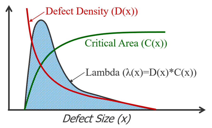
So, how does CAA help? CAA is a set of defect data combined with an analytical tool that lets designers and foundry engineers determine (before actual manufacturing starts) if any given design is likely to have yield problems in manufacturing caused by layout-dependent effects—geometries in a particular configuration that create a susceptibility to manufacturing defects. That generally means, in simpler terms, opens and shorts. Other physical failure points, such as via and contact failures, can also be incorporated into the CAA process.
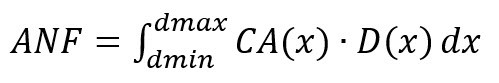
Where does that data come from? Foundries keep close tabs on the number of physical failures associated with their manufacturing processes, so they can adjust and improve their processes to reduce their defect occurrence rate. After all, producing good die is why they’re in business. They also provide this defect density data to EDA companies, who incorporate it into CAA tools (like the Calibre YieldAnalyzer tool) that can be used by design engineers to check their designs for potential manufacturing trouble spots. Once a design has been analyzed, designers can use the results to adjust their layouts as needed before delivering them to the foundry. Removing these potential defect sites before manufacturing helps improve both yield ramp and overall yield. Win-Win! Couldn’t get enough of statistics and equations in college? You’ll love CAA! Get a more detailed explanation of how CAA works in our white paper, Getting Started with Critical Care Analysis. Hated statistics? Download the paper anyway—we use lots of words and pictures, too, to describe how CAA does what it does. Understanding and adopting CAA can help you make those final design changes with confidence, and improve your chances of achieving the desired yields.