Smoothing the path to manufacturing success begins with CMP simulation and fill optimization
By Ruben Ghulghazaryan, Davit Piliposyan, Zhengfang Liu, Chunshan Du, Jeff Wilson, Qijian Wan, Xinyi Hu, Zhixi Chen
Chemical-mechanical polishing (CMP) is a key process in integrated circuit (IC) manufacturing, used to ensure surface planarity. Successful fabrication and performance of semiconductor devices is highly dependent on the final planarity of the processed layers. CMP engineers strive to optimize design planarity, but the variety of available fill options typically requires expensive and time-consuming wafer production to determine the best solution.
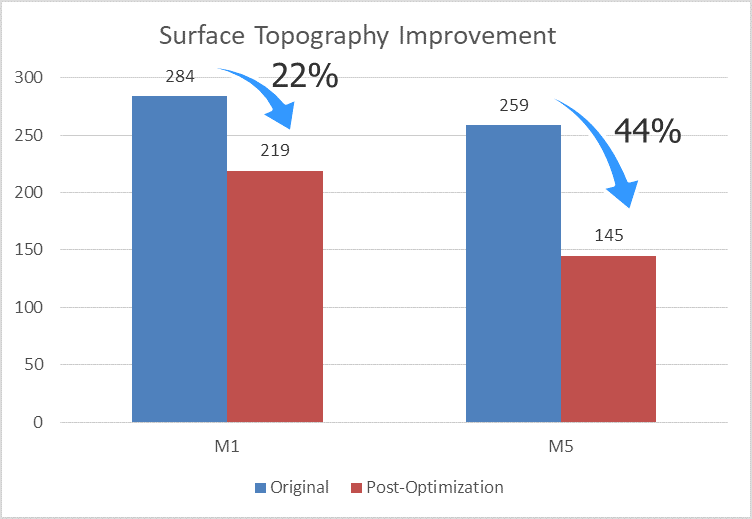
Siemens EDA and Huali Microelectronics joined together to conduct a joint project to determine how effective it would be to use CMP modeling and simulation in conjunction with automated fill placement to analyze designs before manufacturing to predict post-CMP planarity, identify potential hotspots, determine the optimal fill pattern, and remove and replace fill to achieve the most efficient planarity compliance solution. As you might guess from the chart at the top, our results demonstrated that using CMP simulation for both post-CMP hotspot detection and dummy fill pattern selection provides a faster and more precise dummy fill optimization, which improved hotspot fixing and increased compliance with surface planarity requirements.
The general flow is as follows:
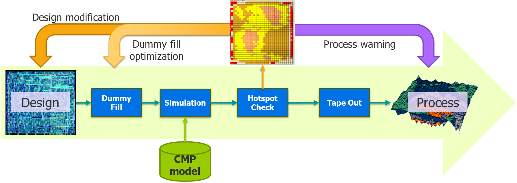
- For a given layout, insert a dummy pattern using a rule-based dummy fill deck with the Calibre YieldEnhancer SmartFill functionality.
- Run CMP simulation and detect hotspots based on the rules and threshold criteria for a given process.
- If hotspots are detected, run the Calibre CMPAnalyzer hotspots clustering algorithm to detect and group hotspots to ease the hotspot fixing process. If no hotspots are found, save changes and move to the next step in the design flow.
- Run a hotspots fixing flow using model-based SmartFill functionality that fixes the hotspots using dummy pattern modification based on the CMP simulation results.
- For the selected area or cluster, use the engineering change order (ECO) flow in the Calibre YieldEnhancer SmartFill tool to control the removal of the original dummy fill.
- Refill just these areas with new dummy fill shapes selected based on analysis of the hotspot type (such as large dishing or erosion, low or high topography, surrounding pattern density, density gradient, design rule constraints, etc.)
- Repeat CMP simulation and check for hotspots.
We tested this flow for back-end-of-line layers on a design with five layers (M1-M5), resulting in significant planarity improvements without the need for test wafer production. You can learn more about the details of the process, and see all the results we achieved, in our technical paper, CMP Simulation-Based Dummy Fill Optimization.