How Mentor is Helping You Make Silicon Photonics a $1.3B market by 2022
By Michael Buehler-Garcia, Senior Director, D2S Calibre Marketing – Mentor, A Siemens Business
Companies who want to explore the potential of silicon photonics can depend on Mentor tools and processes to help them succeed.

There’s been quite a rising and accelerating rumble about silicon photonics being the next new wave of growth for the IC design community, with analyst firms predicting the market could jump up to $1.3B by 2022. By definition, any projection that has a date and dollar amount is going to be wrong, but Mentor® and our design flow partners in silicon photonics have made great progress in establishing a silicon photonics design flows that offers a solid, reliable path to chip manufacturing.
Of course, you can find a number of resources to explain silicon photonics in greater detail, but the fundamental promise of silicon photonics is to improve overall systems performance by taking the fiber-optic speed-of-light communications lines that connect a growing number of communications systems (typically in long-haul networking and cable communications) and bringing that technology right onto the chips. Eliminating or reducing the connection to copper and its related latency between connected devices, whether those devices are on your personal computer, your set top box, the server at your bank, or the many, many connections between all of them, will make everything faster, while at the same time reducing power. And of course, in the electronics biz, we all know faster with lower power is better.
Over the last six years, Mentor and our partners in silicon photonics have made great progress on developing silicon photonics design flows and a path to better manufacturing. Moreover, we have implemented inventive licensing programs to nurture silicon photonic development from academic experiments into broader commercial deployment.
On the design front, Mentor partnered very closely with PhoenIX Software BV, Lumerical Solutions, VPIphotonics, and various research institutions to develop a physical design to manufacturing flow for photonic integrated circuits (PICs). In the flow, PIC design teams (composed of physicists and EEs) use PhoeniX OptoDesigner with one of Mentor’s custom layout tools to develop the layout of the PIC. They then use the Calibre® platform to perform both design rule checking (DRC) and layout vs schematic (LVS) design verification, along with planarity analysis, automatic and intelligent fill insertion, and chip finishing. Precise fill insertion is particularly important with PIC, as a significant amount of the light travels outside to the waveguides! Designers can also use the Calibre LFD lithographic simulation tool to predict how both wave guides and switches will look as manufactured. These as-manufactured shapes can then be fed into optical simulators like Lumerical to estimate performance.

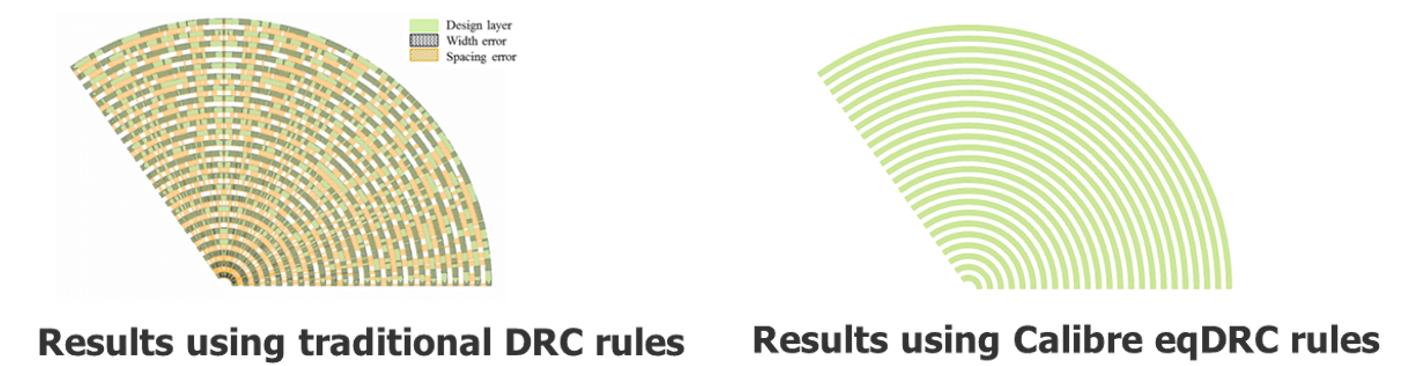
It’s important to note that physical design of PICs is more akin to custom radio frequency (RF) layout than traditional digital layout. Photonic features on a PIC are non-Manhattan—they are often curvilinear, or include angles other than 90°. Design tools must be able to accommodate freehand placement of PIC building block features—such as ring resonators, grating couplers, delay lines, and arrayed waveguide gratings. Physical verification of these non-Manhattan shapes, and manufacturing of these features in nanometer process geometries, is extremely complex. The DRC solution must be able to properly and accurately check curved designs. Using the Calibre eqDRC™ equation-based capability within the Calibre nmDRC™ platform, we have been able to significantly reduce false errors.
Over the last several years, Mentor has worked with research organizations, Mentor OpenDoor® software partners, and select foundries to extend the functionality of many tools in the Calibre platform to ensure PIC design teams can send clean designs to manufacturing and that yield will be optimal.
From parasitic extraction through lithography simulation, LVS, DRC, and even yield analysis, we have developed multiple new verification features and capabilities to ensure there is a silicon photonics design flow ready for production manufacturing.

What’s more, we have also worked with research organizations like CMC Microsystems in Canada to offer licensing terms that gives academics and PIC startups access to no-cost licensing of the Mentor PIC flow while doing initial design prototyping and research. By enabling these companies to experiment with and develop their PIC processes, Mentor is helping to ensure that the resulting products and processes successfully move to production, supporting the overall growth of the PIC industry and the new and exciting products it can offer.
References
[1] X. Wang et al., “Lithography simulation for the fabrication of silicon photonic devices with deep-ultraviolet lithography,” The 9th International Conference on Group IV Photonics (GFP), San Diego, CA, 2012, pp. 288-290. doi: 10.1109/GROUP4.2012.6324162

Want to Know More?
Intro to Silicon Photonics:
Silicon Photonics and Lithography:
http://www.techdesignforums.com/practice/technique/silicon-photonics-lithography/