Learn about Aprisa Digital IC Implementation from real users
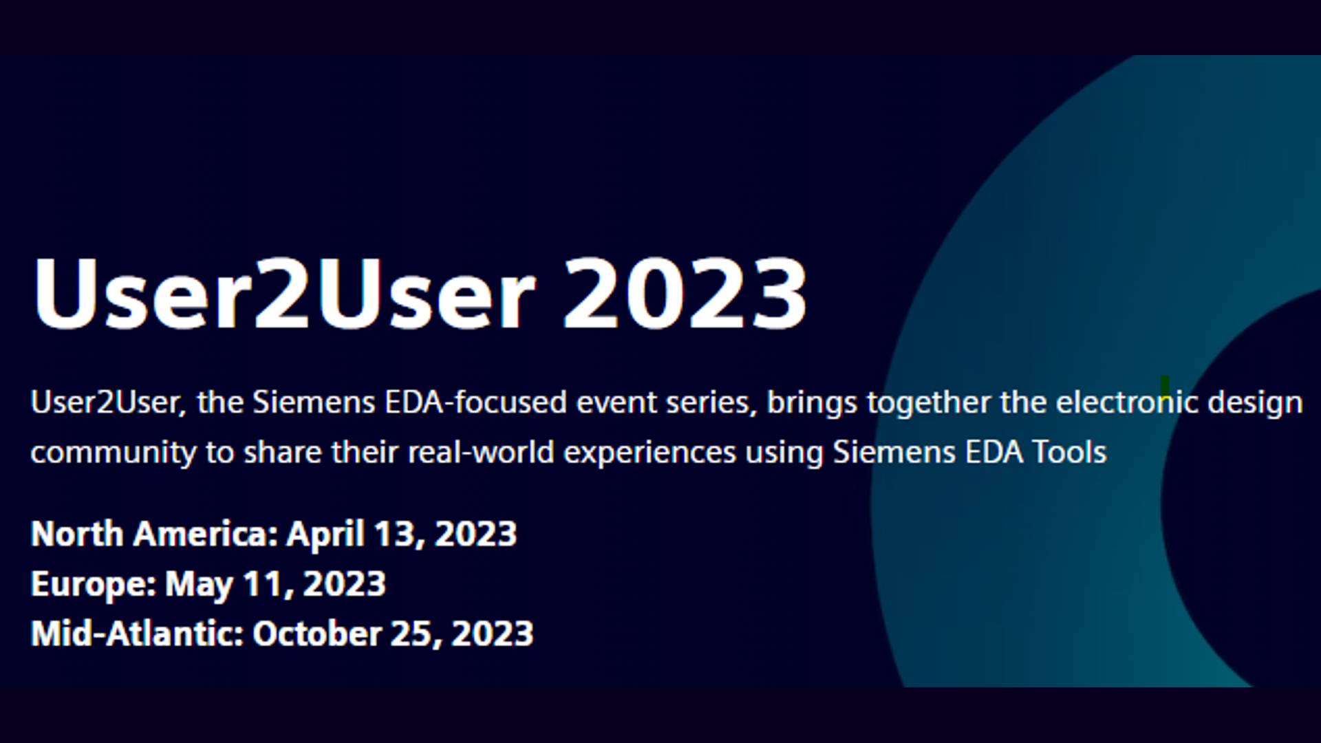
At the 2023 User2User North America symposium, real users dished on using Aprisa
Siemens’ place and route solution was featured in presentations from users like MaxLinear, Arm and indie Semiconductor, who shared their experience using Aprisa on their designs.
The Aprisa track included customer-led sessions showcasing ease-of-use and great out-of-the-box results:
- “How to achieve optimal PPA at placement and carry it through to signoff” presented by Ravi Ranjan, the director of physical design at Maxlinear
- “Implementation of big infrastructure designs” presented by Roma Rudra, technical director at Arm
- “Experiencing the benefits of Aprisa, and the partnership with Siemens design services” presented by Sean Kao, senior principal engineer at indie Semiconductor
Ravi Ranjan presented “How to achieve optimal PPA at placement and carry it through to signoff.” MaxLinear is a leading provider of radio frequency (RF), analog, digital, and mixed-signal integrated circuits for access and connectivity, wired and wireless infrastructure, and industrial and multimarket applications. This session covered Maxlinear’s experience in the adoption of Aprisa for designs in 16 nm and 5 nm technologies. Ravi shared how his team found that Aprisa provides an easy-to-use flow with excellent correlation and integration to third-party extraction and STA tools.
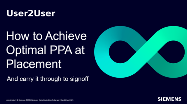
More compelling for Maxlinear has been Aprisa’s salient features—its ability to maintain timing throughout the placement, CTS and post-route phases, all while achieving optimal performance, power, area (PPA). In addition, Maxlinear also values the fact that Aprisa does not require module place grouping, which eases the burden on their designers during the P&R flow.
Aprisa has a detail-route-centric architecture. That means that the routing information and parasitics are available to all engines throughout the flow. This is important because at advanced nodes, the layers are uneven, the RCs are different, and therefore the P&R tool needs to understand the layer assignments, net topologies and number of vias starting as early as placement. Knowing this information starting at placement gives better correlation throughout the flow which leads to fewer iterations, fewer ECOs, and faster tapeouts.
Attendees will heard from Roma Rudra, a technical director at Arm about the “Implementation of big infrastructure designs.”
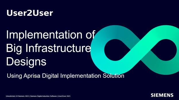
Arm silicon partners ship over 20 billion Arm-based chips every year, which are found in smartphones, computers, televisions, smart cars, wearable technology, and more recently servers. Roma will share her team’s experience using Aprisa to implement a Compute Subsystem (CSS). A CSS aims to deploy systems built around Arm IPs for the infrastructure market targeting Enterprise, HPC, Cloud and Edge servers. These are large to very large systems comprising of as many as 128 Arm cores in a monolithic die operating at >2.5GHz on leading process nodes. Roma described the approach and challenges to implement such large systems, and how Aprisa addresses those challenges through its tight correlation throughout the flow, and minimal need for guidance required to achieve optimal results.
Aprisa has intrinsic intelligence resulting in a single reference flow, giving IC designers great out-of-the-box results. Aprisa can use one reference flow to support multiple blocks, projects and designs with very minimal additional guidance. Aprisa works with no to minimal need for placement groupings, clock tree synthesis (CTS) guidance, and R/C scaling. It’s foundry ready, and tapeout proven.
The advantages of out-of-the-box tapeouts are that they lower the cost of tool ownership, reduce reliance on power users for custom recipe generation, allow better scale engineering and use of CAD resources, and meet optimal PPA for small and large designs at any nodes, faster and with fewer iterations.
The third customer presentation, “Experiencing the benefits of Aprisa, and the partnership with Siemens design services”, came from senior principal engineer at indie Semiconductor, Sean Kao. indie Semiconductor brings cutting edge semiconductor and software solutions for automotive applications focusing on three key areas: advanced driver assistance systems (ADAS), in-cabin user experience (UX), and electrification. indie has found a reliable partner in Siemens digital implementation services for driving program management and ASIC physical design execution. The CLS (Consulting and Learning Services) team at Siemens uses Aprisa as a tool for rapid and robust digital IC implementation. With close cooperation and coordination between the two engineering teams from indie Semi and Siemens, design challenges were effectively and efficiently analyzed and overcome.
Join us and find out for yourself!